
40MHz 32 Channel PC-Based Logic Analyser

The 32-channel, 40 MHz logic analyzer is designed for versatile applications in digital circuit testing and debugging. It supports TTL and CMOS logic levels, making it suitable for a wide range of digital devices. The analyzer’s capability for both internal and external triggering allows users to capture signals based on specific conditions, enhancing its utility in complex debugging scenarios. The maskable internal triggering feature enables users to selectively monitor specific signal levels across all channels, providing flexibility in signal analysis.
The logic analyzer is implemented on a single-sided PCB, which minimizes assembly complexity and enhances reliability by reducing the potential for wiring errors. However, users must be prepared to fabricate the PCB themselves, as complete kits are no longer available. The programming of the PLDs is a crucial step in the assembly process, as these devices are initially blank and require the appropriate JED files to be functional. The availability of internal schematics aids users in understanding the configuration and functionality of the PLDs, facilitating the programming process.
The reported issue with the timebase generation circuit is significant for users relying on accurate frequency measurements. The incorrect output frequency from the Q1 pin of IC4 necessitates a careful examination of the circuit design and may require modifications to ensure proper clock generation. Users may need to implement corrective measures to address the clock frequency discrepancy, particularly if they are working within the 10 MHz range or lower.
In summary, while the 32-channel, 40 MHz logic analyzer presents a valuable tool for digital analysis, potential builders must possess the requisite skills to fabricate the PCB, program the PLDs, and troubleshoot any issues that may arise during the assembly and operation of the device.It is a 32 Channel, 40Mhz, fully PCcontrolled TTL/CMOSlogic analyser with internal/external triggering and trigger delay. Internal triggering is fully maskable (High/Low/Don`t Care) on all 32 channels. The whole things fits on one single sided PCB with virtually no wiring! Unfortunately the PCLA is not available as a complete kit from any of the k it suppliers, and I no longer sell the pre-programmed PLD`s. Only the software is available. So if you want to build it, then I`m afraid you`ll have to make the PCB and program the PLD`s yourself. The PLD`s were designed with the old Lattice Semiconductor ispLSI starter kit, but the newer Lattice development tools are available from the lattice web site.
I have not used this new software, and email reports indicate that the files on this page are not compatible with it. I do not know how to solve this issue, so please don`t ask. I have no plans to upgrade this project to new devices or software. The internal schematics for the chips are available on this page, you can use these to program the newer devices yourself.
NOTE : I get a *lot* of email about the ispLSI PLDchips in this project. For those of you who are unaware of what they are, they are Programmable Logic Devices, and they are BLANK when you buy them, you MUSTprogram them with the JED files from here in order to get them to work. If you don`t even know this much then you really have no need for this project! Peter Baxter has developed a new Logic Anlyser product that should be on the market around the end of 2003.
The delay is due to Business Partner issues, rather than engineering aspects. The earlier kit version completely sold out in 1999. There are no units available and no spare parts. You can look at the website: for info on the kit, but don`t get excited by it. It is closed. The new one will be worth the wait. There is a problem with the timebase generation circuit that causes the 10MHz and lower ranges to be inaccurate. The basic problem is that the Q1 output of IC4 does not produce a 10MHz clock, but 8MHz instead, which causes all the ranges 10MHz and below to have an inaccurate timebase.
🔗 External reference
Related Circuits
The design of the digital logic probe centers around a pair of complementary bipolar transistors, which, in this application, are used as electronic switches. The digital logic probe is a diagnostic tool utilized for testing and analyzing digital circuits. The...
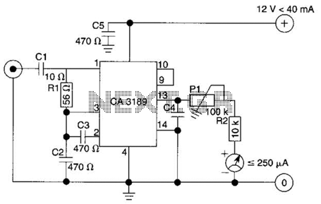
4-channel SQ logic decoder with a current drain of 75 mA at 20 volts. The input impedance is 2M ohms, and the output impedance is 2K ohms (courtesy of GTE Sylvania Incorporated). The 4-channel SQ logic decoder is an integrated...
These two simple circuits provide zero voltage switching. They can be used with full wave bridges or in antiparallel to provide full wave control and are normally used to trigger power thyristors. If an input signal is present during...
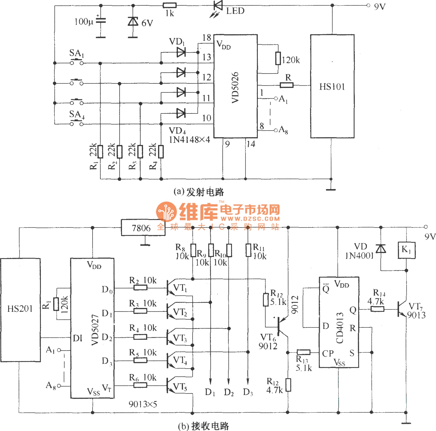
HS101 and HS201 are small radio transceiver components operating at a frequency of 280 MHz, designed for digital signal transmission. They provide a control distance ranging from 30 to 100 meters. All components, including the antenna, are integrated into...
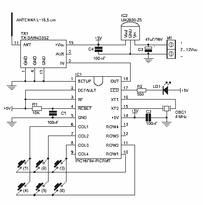
This project creates a simple but valuable wireless remote controller. It has as many as 6 channels (a rare feature for remote control devices) and transmits encoded MM53200, UM3750, or UM86409. Of course, you can omit the button and...

Logic overvoltage protection power supply. Refer to the designated page for an explanation of the power supply circuit diagram mentioned above. The logic overvoltage protection power supply is designed to safeguard sensitive electronic components from voltage spikes that could potentially...