
500A power switch control circuit diagram

The circuit design utilizes 50 BUZ23 FETs, which are configured in a parallel arrangement to enhance current handling capabilities while maintaining a blocking voltage of 100V. The choice of BUZ23 transistors is significant due to their low on-resistance and high switching speed, which contribute to efficient operation in high-current applications. The minimal control power requirement is a key feature, as it reduces the energy consumption associated with driving the gates of these transistors. This characteristic also mitigates the risk of thermal runaway and second breakdown, which are critical concerns in high-power electronics.
In this configuration, the gate resistance is strategically selected to ensure that the gate drive signals are adequately delivered to all 50 transistors without introducing significant delays or losses. The parallel arrangement allows for the distribution of the gate drive current, thereby minimizing the impact of each individual transistor's gate capacitance on the overall circuit performance.
The inclusion of 20 parallel RC absorption circuits plays a vital role in managing the inductance inherent to the circuit wiring. These RC circuits serve to dampen voltage spikes and transients that can occur during switching events, effectively protecting the FETs from potentially damaging conditions. The RC absorption circuits are designed to absorb excess energy that may be stored in the inductive components of the circuit, ensuring stable operation and prolonging the lifespan of the transistors.
Overall, this circuit design exemplifies a robust approach to managing high currents in a compact form factor while maintaining reliability and efficiency. The careful selection of components and their arrangement is crucial in achieving the desired performance characteristics in high-power applications.The circuit uses 50 BUZ23 field effect transistors connected in parallel, tube blocking voltage of 100V. Required control power is extremely small, and there will be no second breakdown and conduction zone positive temperature coefficient phenomenon.
As the entire circuit current is large, it is where the gate resistance, using the connection element 50 in parallel. In order to load circuit wiring inductance let go of the energy stored in the drain - source access between the 20 parallel RC absorption circuit elements.
Related Circuits
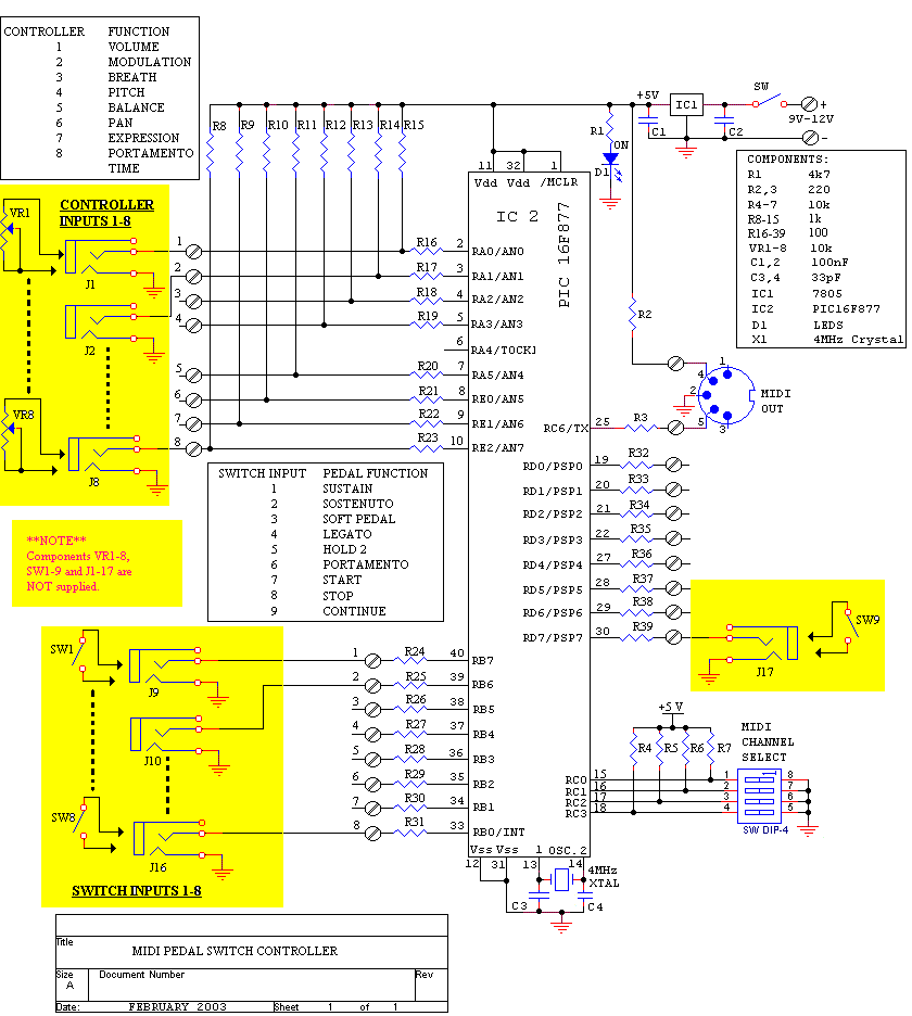
The sustain pedal, also known as the damper pedal, sends a controller value of CC64 when operated. Pressing the pedal results in an output value of 127, while releasing it results in an output value of 0. Tone generators...
As the market seeks lighter, more compact wireless and portable devices with innovative features packed into increasingly constrained spaces, there is a concurrent pursuit for the next power supply innovation—a powerful, compact, long-lasting, economical, and safe battery. Although advancements...
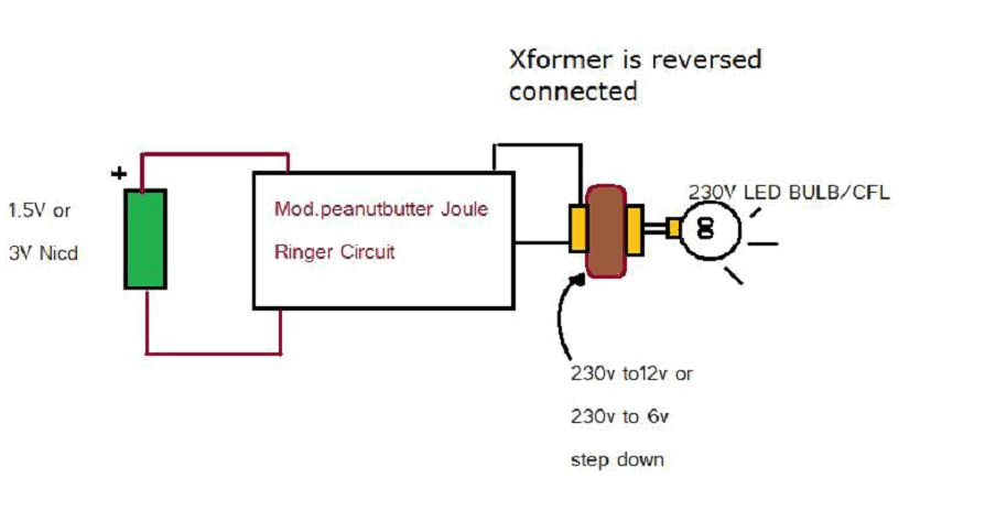
Various threads on ringer circuits have been observed, showcasing multiple variants, particularly concerning the types of transformers utilized, such as air core and step-down transformers. One notable circuit is the 12V-to-120V configuration, which employs a joule ringer that utilizes...

At dawn, light illuminates the photosensitive resistor RL, causing its resistance to decrease. This switch IC (2) exhibits a high electrical footprint. When light is present, the relay K does not activate. At night, in the absence of light,...
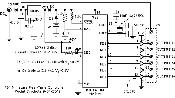
The F84 MRTC was my second design of a miniature real-time controller. This version uses PIC16F84 running with a low power X-tal 32,768Hz. The scheduler for 6-channel output was saved in EEPROM. No terminal for serial downloading of the...
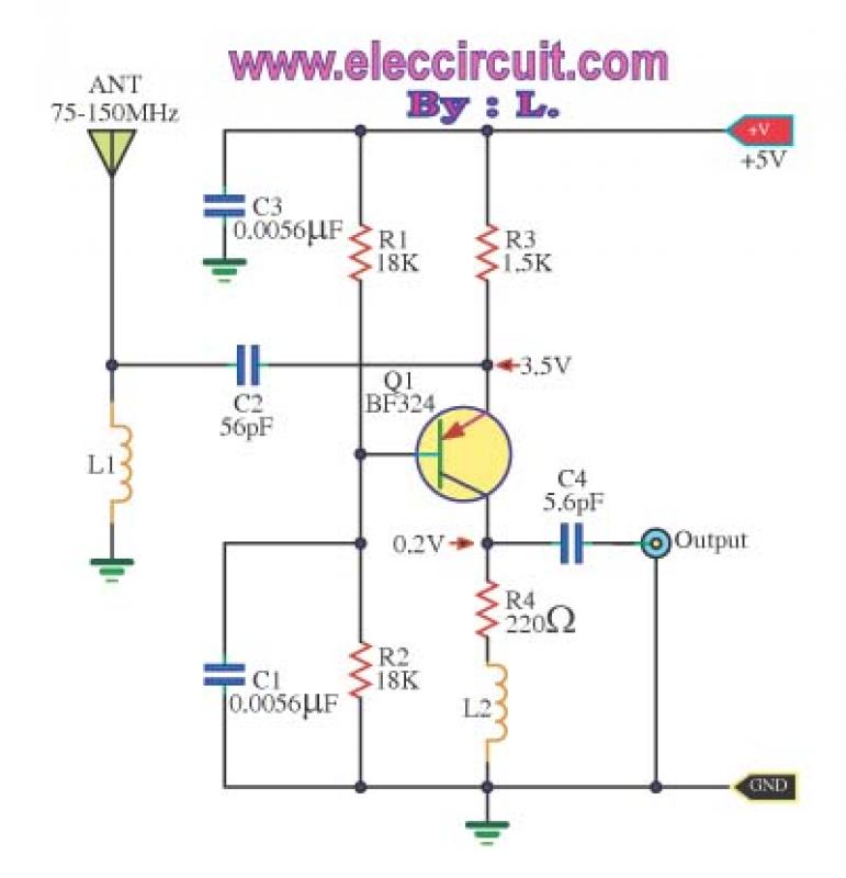
This is a wideband high-frequency amplifier circuit designed for a frequency range between 75-150 MHz. It utilizes a PNP transistor amplifier to enhance signal strength before it reaches the receiver of devices such as phones, FM radios, or amateur...