
50W class AB amplifier

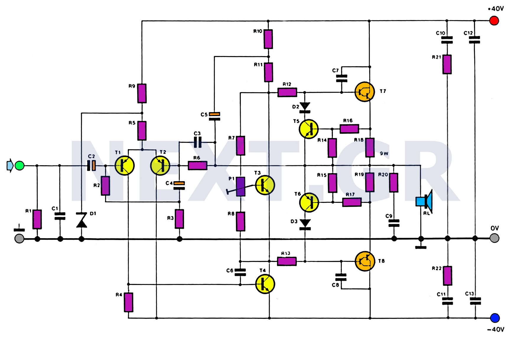
The described pure Class AB output stage amplifier circuit is designed to provide a balance between performance and simplicity, making it an attractive option for enthusiasts and professionals alike. The differential amplifier formed by transistors VTI and VT4 allows for effective signal amplification while minimizing distortion. The choice of components, particularly the power output transistors VT6 and VT7, is crucial for achieving the desired output characteristics, including linearity and thermal stability.
To further elaborate on the circuit's operation, the biasing network involving diodes VD1, VD3, and VD5 plays a vital role in ensuring that the output transistors operate in their optimal range, thus enhancing the overall fidelity of the amplifier. The resistors R6 and R7 not only control the gain but also help in setting the input impedance of the amplifier, which is essential for matching with various audio sources.
The adjustment process outlined is critical for fine-tuning the amplifier's performance. Setting the midpoint potential to 0V with RP1 ensures that the amplifier operates in a balanced state, preventing crossover distortion. The adjustment of RP2 to achieve a voltage of approximately 0.1V across R13 is indicative of the quiescent current flowing through the output stage, which is key to maintaining the Class AB operation without significant thermal runaway.
Overall, this amplifier circuit represents a practical solution for those looking to build a high-quality audio amplifier without delving into overly complicated designs. The straightforward nature of the circuit, combined with the clear adjustment procedures, makes it accessible for both novice and experienced builders.Fans are hoping to make a high-quality amplifier, but the most outstanding publications published on the circuit, they often too complex and difficult to start 6 This article d escribes a pure class AB output stage amplifier circuit, the circuit is simple, sound quality is satisfactory, Hing interested persons may wish to try the heart of the circuit shown in Figure 4-3. VTI ~ VT4 composed of one, two differential amplifier, VT6 ~ VT7 constitute power output tube, VT8VT9 to promote o VDl --VD3VT5 circuit providing a bias to VT6 ~ VT9.
Gain of the circuit by the R6, R7 control about 30 times. The entire circuit is simple and clear, at a glance. Adjustment of the machine is very simple: to make the midpoint potential of adjustments RP1 ov; adjust RP2, so that the voltage across R13 is about 0.1V. Several times repeated adjustments can be put into use
Related Circuits
This amplifier is designed with the following specifications: distortion less than 0.1% at full power of 100W even at 20KHz, with power attributed to an extended bandwidth. The output transistors are protected against short circuits, and the power supply...
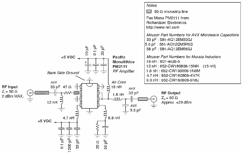
RF Power Amplifier 1 Watt. Jams Cellular Downlink Band: 800-950 MHz. The RF power amplifier described is designed to operate within the cellular downlink frequency range of 800 to 950 MHz, delivering an output power of 1 Watt. Such amplifiers...
This versatile amplifier circuit was designed and submitted by Mr. Seetharaman Subramanian from Chennai. The original concept appeared in Practical Electronics, a UK-based magazine, and the circuit was finalized after extensive field trials and modifications between 1981 and 1986....
The diagram below illustrates that power supplies need not be complex, particularly in low-power applications. The filaments are powered directly from the 120-volt AC line, minimizing the size of the transformer(s) required to drive the amplifier. Note the slightly...

The audio power amplifier delivers 80W of audio power to an 8-ohm load. The LM3875 integrated circuit (IC) requires adequate cooling. It is important to note that in the bridge amplifier configuration, the two connected speakers will produce heat. The...

TV RF Power Amplifier 14W. This RF power amplifier operates within the frequency range of 470 - 860 MHz, covering UHF Band IV and V, and delivers an output power of 14 Watts with an input power of 1.5...