
Phone Jammer linear amplifier

The RF power amplifier described is designed to operate within the cellular downlink frequency range of 800 to 950 MHz, delivering an output power of 1 Watt. Such amplifiers are crucial in communication systems, particularly for enhancing signal strength in various applications, including jamming scenarios.
The amplifier typically consists of several key components: a transistor, which serves as the active device for signal amplification; biasing circuits to set the operating point of the transistor; impedance matching networks to ensure efficient power transfer between stages and to the load; and a heat sink for thermal management, as power amplifiers generate significant heat during operation.
In the context of jamming, this amplifier would be used to disrupt communication signals within the specified frequency range. The design would need to incorporate features that allow for stable operation under varying load conditions and the ability to handle high-frequency signals without distortion.
The input stage may include a low-noise amplifier (LNA) to boost the incoming signal before it is processed by the main amplification stage. Following amplification, a filtering stage is often employed to suppress unwanted harmonics and ensure that the output signal remains within the desired frequency band.
Power supply considerations are also critical, requiring a stable DC supply that can handle the current demands of the amplifier. Additionally, protection circuits may be included to prevent damage from over-voltage or over-current conditions, ensuring reliable long-term operation.
Overall, the design of an RF power amplifier for jamming applications involves a careful balance of performance, efficiency, and reliability, suitable for the intended operational environment.RF Power Amplifier 1 Watt. Jams Cellular Downlink Band: 800-950 MHz. 🔗 External reference
Related Circuits
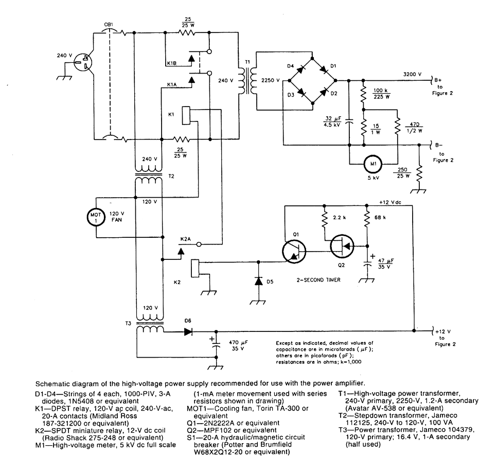
A schematic diagram of the high-voltage power supply recommended for use with the power transformer. This power supply can also be used for other equipment with similar requirements. CAUTION: hazardous high voltages. The high-voltage power supply schematic is designed to...
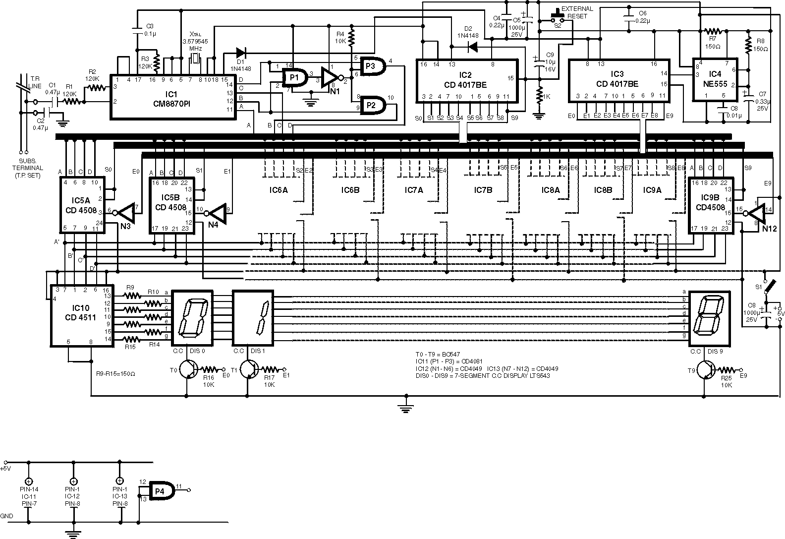
The given circuit, when connected in parallel to a telephone, displays the number dialled from the telephone set using the DTMF mode. This circuit can also show the number dialled from the phone of the called party. This is...
This project utilizes the IRF510 MOSFET, a widely available N-Channel enhancement mode power field effect transistor. It is designed to withstand specified levels of energy in breakdown avalanche mode. Unlike bipolar transistors, which are current-controlled and have lower input...

Inspect the work for potential dry joints, shorts across adjacent tracks, or soldering flux residues, as these often lead to issues. Recheck all external connections to and from the circuit for any mistakes. Ensure that all polarized components are...

RTD sensors are measured using a precision 24-bit analog-to-digital converter (A/D) that includes a built-in programmable gain amplifier. The connections for 2-wire, 3-wire, and 4-wire RTDs are illustrated. This setup facilitates the connection and measurement of RTDs with amplifiers and...
The transistor Q1 and its associated components form a tunable RF oscillator. The RF signal is directed to transistor Q2, which functions as the modulator. Operational amplifier IC1 amplifies the audio signal and transmits it through resistor R4 to...