
51 surround amplifier circuit schematic

The 5.1 surround amplifier circuit based on the AN7168 IC is engineered to provide an immersive audio experience, making it suitable for home theater systems. The AN7168 is a versatile integrated circuit that can drive multiple channels of audio, making it ideal for creating a surround sound environment. The circuit's design supports five channels of amplification, allowing for the connection of left, right, rear left, rear right, and center speakers, which is essential for a true 5.1 surround sound system.
The recommended operating voltage of 12V ensures that the circuit remains within safe limits for the components, while still delivering adequate power. The option to increase the voltage up to 24V allows for greater output power, enhancing the overall sound performance, particularly in larger spaces or when higher volume levels are desired. However, care must be taken not to exceed the voltage ratings of the components to avoid damage.
The amplifier is capable of delivering a maximum power output of 40W at an impedance of 4 ohms, making it suitable for driving standard home audio speakers. The circuit's design must ensure that the impedance of the connected speakers matches this specification to achieve optimal performance and prevent any potential damage to the amplifier.
For a complete 5.1 surround sound experience, it is necessary to construct five separate amplifier circuits, one for each speaker channel. This modular approach allows for flexibility in system design and enables the user to customize the setup according to their specific audio requirements. The subwoofer, which plays a critical role in low-frequency sound reproduction, should be powered by a separate subwoofer amplifier designed to handle the unique demands of subwoofer speakers.
In conclusion, the 5.1 surround amplifier circuit schematic using the AN7168 IC provides a robust solution for creating a multi-channel audio system, ensuring high-quality sound reproduction across multiple speaker configurations. Proper implementation of this circuit will yield an effective surround sound experience, enhancing the overall enjoyment of audio and video content.This 5. 1 surround amplifier circuit schematic use the IC AN7168 as the main component from this circuit. Minimum voltage required 12V and maximum voltage 24V, I recomended it 12 V because the voltage support on are components. But if you want to better a loud sound you can raise it. Maximum power output 40W with impedance 4 ohm. This 5. 1 surrou nd amplifier circuit schematic also support to make surround sound or 5. 1 speaker. Use this amplifier on rear speaker, left right, and center but dont use to subwoofer speaker. See 5. 1 surround amplifier circuit schematic below : If you want to make a 5. 1 surround sound you must make 5 the circuit of 5. 1 surround amplifier circuit schematic, for left and right speaker, rear left and right speaker, and center speaker. Use the subwoofer speaker with support amlplifier subwoofer circuit. 🔗 External reference
Related Circuits
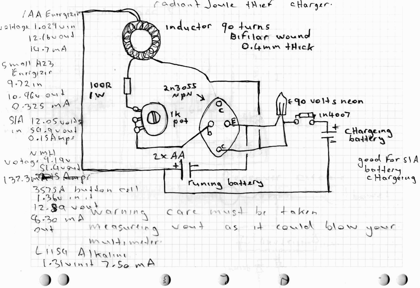
A high power joule thief circuit is explained in this post, which can be constructed by any new hobbyist. Here is the simplified drawing of the radiant joule thief battery charger. The inductor was wound with many turns until...
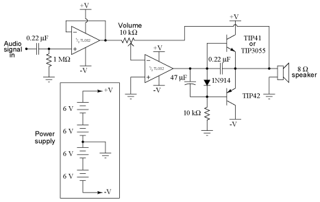
It is advisable to obtain TIP41 and TIP42 transistors, which are closely matched NPN and PNP power transistors with dissipation ratings of 65 watts each. If a TIP41 NPN transistor is unavailable, the TIP3055 (available from Radio Shack) serves...
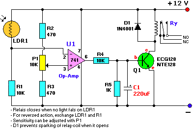
The provided schematic diagram illustrates an LM741 light/dark sensor circuit, derived from the 741 Op-Amp Tutorial by Tony van Roon. The ECG128/NTE128 transistor can be replaced with any NPN transistor that meets the necessary gain and current specifications for...
Charging the battery in a slow manner (using a low charging current over an extended period) is the most economical and safest method. The design of the trickle charger should focus on two key points: firstly, the use of...
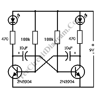
This LED flasher circuit is a classic two-transistor flip-flop. It is a popular circuit often built by beginners in electronic circuit design. The schematic diagram of this well-known LED flasher circuit consists of two transistors, two capacitors, four resistors,...
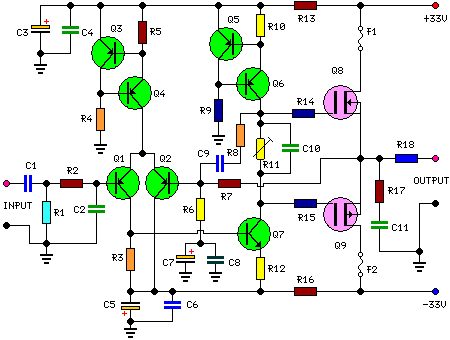
This is a 25-watt basic power amplifier designed for ease of construction at a reasonable cost. It outperforms the standard STK module amplifiers commonly found in mass-market stereo receivers today. The design was initiated to create a 25-watt amplifier...