
555 based Voltage inverter Schematic

The described circuit is a voltage inverter that employs a charge pump topology. It typically consists of capacitors, diodes, and a switching element, such as a transistor or an integrated circuit (IC), to achieve the voltage conversion. The operation principle relies on the charging and discharging of capacitors to create a negative output voltage relative to the ground.
In a standard configuration, the circuit begins with a positive input voltage applied across a capacitor. During the charging phase, the capacitor stores energy. When the switch toggles, the stored energy is transferred through a diode to another capacitor, which is connected to the output. This process effectively inverts the voltage, resulting in a negative output while accounting for the voltage drop across the components.
To utilize the circuit as a voltage doubler, the output can be connected to the ground reference of a subsequent circuit. This configuration allows for the effective doubling of the input voltage, providing a higher voltage output for applications requiring increased power levels.
The design must consider factors such as the frequency of operation, component ratings, and load requirements to ensure efficiency and stability. Additionally, filtering capacitors may be employed at the output to smooth the voltage ripple, enhancing the performance of the circuit in sensitive applications. Proper layout and grounding techniques are essential to minimize noise and ensure reliable operation in various electronic environments.This circuit will convert a positive voltage to a negative voltage, while losing 1. 5 V (approximately). For example, if you`re supplying 9V to the circuit, the output will be -7. 5 V. This circuit can also be used as voltage doubler, by using the output as the new ground for another circuit. 🔗 External reference
Related Circuits
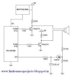
A horn driver project developed by Microchip Technology is illustrated in this circuit diagram. This horn driver project utilizes the PIC16F886 microcontroller from Microchip. The circuit diagram for the PIC microcontroller horn driver is straightforward and requires minimal external...
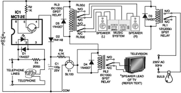
A telephone line-based audio muting and light activation circuit. Frequently, when listening to music or watching television at elevated volume levels, it becomes difficult to hear a telephone ring, resulting in missed important calls. This circuit is designed to address...
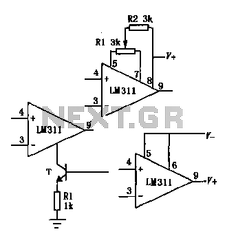
The LM111/211/311 power supply operates within a voltage range of 5V to 15V. It features bias current, offset current, and a differential input voltage range of 30V. The output is compatible with TTL, DTL, and MOS circuits, allowing it...
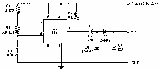
This circuit inverts the polarity of the input. Output is limited to less than 200mA. More: U1 NE555 timer IC R1 1.2k ohm resistor R2 3.9k ohm resistor R3 1k ohm resistor C1 0.05 uF ceramic capacitor C2, C3...
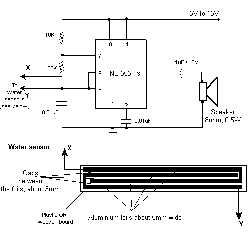
This weblog discusses electronic circuit schematics, PCB design, DIY kits, and electronic project diagrams. The rain detector operates on the principle of an astable multivibrator using the 555 timer IC, which is equipped with a sensor capable of detecting...
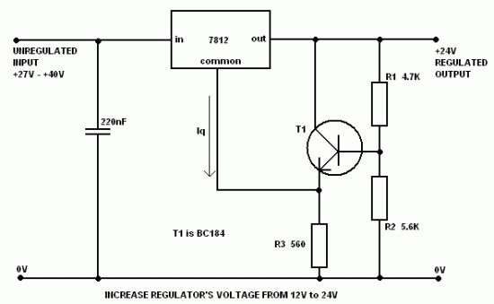
It is often necessary to configure a voltage regulator integrated circuit (IC) to provide a higher output voltage than that established by the regulator alone. One method to achieve this is by connecting the common terminal to the midpoint...