
555 tone generator circuit

The circuit under discussion employs two 555 timers configured as astable multivibrators, generating pulse signals that can be summed or manipulated through an operational amplifier. The astable configuration of the 555 timer is characterized by a continuous oscillation between high and low states, determined by the resistor-capacitor (RC) network formed by R1, R2, and C1. The output frequency (f) of the 555 timer in astable mode can be expressed as:
\[ f = \frac{1.44}{(R1 + 2R2) \cdot C1} \]
This frequency is crucial for applications requiring specific timing intervals or pulse widths. The addition of an operational amplifier allows for the summation of the outputs from the two timers, which can be beneficial in applications such as signal processing or waveform generation.
In the summing configuration, the outputs of the two 555 timers are fed into the input terminals of the operational amplifier. The summing amplifier can be designed to provide a specific gain, allowing for the adjustment of the output voltage level relative to the combined input signals. The output voltage (Vout) can be calculated based on the input voltages (Vin1, Vin2) and the resistor values connected to the Op Amp, following the summing amplifier formula:
\[ V_{out} = -\left( \frac{R_f}{R_1} \cdot V_{in1} + \frac{R_f}{R_2} \cdot V_{in2} \right) \]
where \( R_f \) is the feedback resistor and \( R_1 \) and \( R_2 \) are the resistors connected to each input. This configuration allows for versatile output control based on the input signals, enabling various applications in timing circuits, pulse width modulation, and signal mixing.
In the second part of the circuit, the output of the first 555 timer is utilized to control the operation of the second timer. By connecting the output of the first timer to the reset pin of the second timer, the pulse width of the first timer directly influences the behavior of the second timer. This cascading effect can be effectively used to create complex timing sequences or to generate specific pulse widths for applications requiring precise timing control.
Overall, the combination of two 555 timers with an operational amplifier provides a flexible and powerful solution for generating and manipulating pulse signals in various electronic applications.This circuit takes the outputs from two different 555 multivibrators and combines them using a summing Op Amp. Shown only to depict another implementation of a 555 timer, most of the back ground calculations being covered under the other topics in this section.
The standard configuration for a 555 Astable multivibrator is shown to the left. The ci rcuit is shown again to reference the next schematic which contains two individual astable circuits. Resistors R1 and R2 in combination with capacitor C1 select the output frequency, however the frequency is not relevant to the following discussion [adding two outputs together]. This is one topic of a number covering the 555 timer, with this page covering a combination of 555 timers and operational amplifiers.
The circuit is composed of three ICs; two 555 timers and an operational amplifier. However a dual 556 timer could have been used, but a single 555 timer was used to provide the same pin out given on the other pages covering the 555. The operational amplifier, which is labeled Adder, could be almost any Op Amp including a single, dual or quad package; although only one amplifier is required.
The circuit consists of two individual pulse generators, operating at different pulse widths, and connected to a three input summing amplifier. The third input shows a symbol for a pulse generator, and only depicts the fact that any number of inputs could be used The timers could be set to operate at the same pulse rate, but that couldn`t serve much purpose, as there addition wouldn`t change anything.
The addition of two identical waveform produces the same output as the input, but at a different voltage level. However if the output was required to be at a different voltage level the Vcc could just be taken to a higher voltage, saving the Op Amp.
This is the same circuit used above but configured differently and with out using the Op Amp adder circuit. This circuit generates a single output from two 555 timers concatenated together. Both timers are set up just as all the other astable circuits are, with the resistors and capacitor selected to define the output frequency.
The difference here is that the output of the first circuit feeds into the reset line of the second circuit. So when ever the output of the first timer goes low, the output of the second timer is reset or forced to go low.
This configuration could be changed slightly so that the output of the first stage feeds the threshold of the second stage. The first configuration used the low level of the first stage to force the output of the second stage low, while this second configuration [not shown] uses the voltage level of the first stage to change the output of the second stage.
Either way, both circuit would use the pulse width of the first timer to change the pulse width of the second timer. Note the 555 will not oscillate if RB is greater than 1/2 RA because the junction of RA and RB cannot bring pin 2 down to 1/3 VCC and trigger the lower comparator.
🔗 External reference
Related Circuits
This post presents an interesting topic about switching power supply circuit diagrams for those who wish to learn more. A switching power supply is a type of power supply that uses a switching regulator to convert electrical power efficiently. Unlike...

An LM2808 performs IF amplification of the 4.5-MHz sound subcarrier, limiting, detection, and audio amplification. If the center frequency must be changed, then change L1/C4. Audio output is 0.5 W. R3 is the volume control. The LM2808 is an integrated...
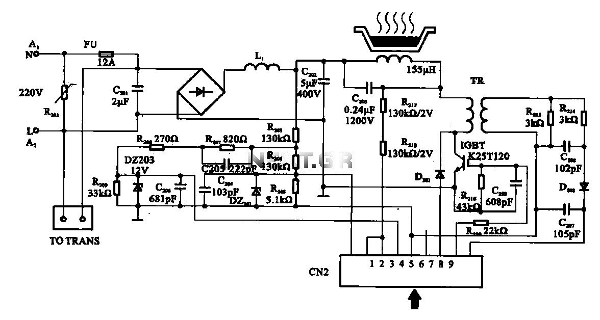
Cooker detection control circuit. The control circuit is designed for testing cookers. The inductance coil disc lesion typically measures around 150 µH. The stove plate coil and capacitor resonate with device C203. When resonating, the voltage generated across C203...
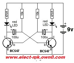
Robot eyes circuit of Service. A simple circuit to simulate a man appointed to it. It consists of a dual-lamp working in an unsteady manner. Circuit diagram. The robot eyes circuit is designed to create a visual effect that simulates...
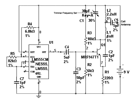
And my recent study about chaos is really making me have FUN! The subject is awesome! And my Geeky Bro informed me something about a cell phone jammer, a simple timer circuit using 555. Will work within 10 feet...
The purpose of this circuit is for research and education. Assistance is sought in acquiring components for simple RF circuits, as well as tutorials or schematics. The requester is facing challenges in locating quality resources for beginner-level RF circuit...