
836MHz low-noise amplification circuit diagram RF2347

The RF2347 is a low noise amplifier (LNA) designed for operation at a frequency of 836 MHz. It is typically used in RF applications where signal amplification is critical, such as in communication systems, RF front-end modules, and various wireless devices. The circuit diagram for the RF2347 LNA includes several key components that contribute to its performance.
The main component of the circuit is the RF2347 IC, which integrates a low noise amplifier with a high gain and excellent linearity. The input stage of the amplifier is designed to minimize noise figure while maximizing gain, making it suitable for receiving weak signals. The circuit also employs impedance matching networks at both the input and output to ensure optimal power transfer and to reduce reflections that can degrade performance.
Additional passive components, such as resistors and capacitors, are used to set biasing conditions and stabilize the amplifier's operation. These components are crucial for ensuring that the amplifier operates within its specified parameters. Bypass capacitors are often included to filter out power supply noise, enhancing the overall performance of the amplifier in a noisy environment.
The power supply voltage for the RF2347 is typically in the range of 3V to 5V, with careful consideration given to the current consumption to maintain efficiency. The output of the LNA can be connected to subsequent stages in the RF chain, such as mixers or additional amplification stages, ensuring that the signal integrity is preserved throughout the system.
In summary, the RF2347 low noise amplifier circuit diagram represents a well-engineered solution for RF signal amplification at 836 MHz, featuring an integrated approach that combines high performance with ease of integration into various applications.836MHz RF2347 low noise amplifier constituting a circuit diagram:
Related Circuits
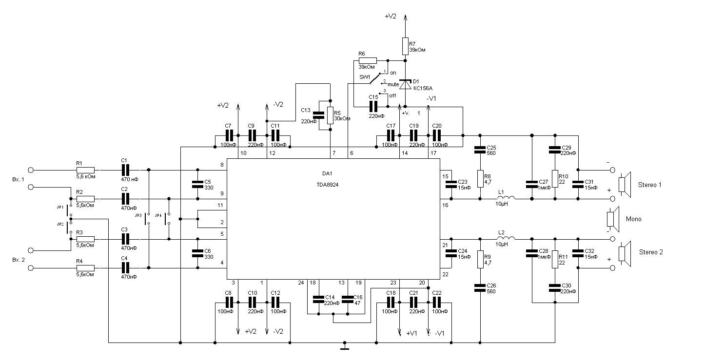
240W power amplifier circuit based on the TDA8924 class D design. This integrated circuit features short-circuit protection at the output, thermal protection, and safeguards against acoustic damage from inrush currents during power on and off. The schematic allows for...
Ensure that connections are verified against the circuit diagram and schematic provided below. This can be utilized while following the tutorial video. The circuit diagram serves as a crucial reference for accurately assembling electronic components in a project. It illustrates...
The cutter is safeguarded by a printed circuit phototransistor designed to prevent accidental activation of the cutter switch during manual feeding. In the event of manual feeding, the automatic paper cutter can be controlled to shut down. A relay...
Expanding schematic circuit for the secondary circuit of high-voltage lines. The schematic circuit for the secondary circuit of high-voltage lines is designed to enhance the distribution and management of electrical power in high-voltage systems. This circuit typically includes components...
The circuit consists of two main components: (1) a power supply circuit featuring a transformer (T) that steps down AC 220V to 33V, followed by a full-wave rectifier, a filter, and a three-terminal regulator that outputs +24V. This circuit...
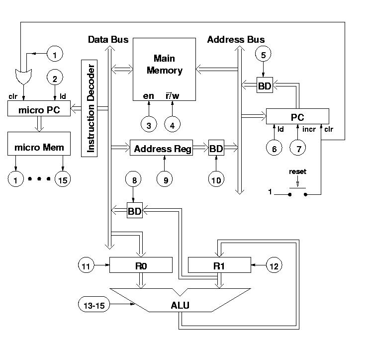
The diagram features a micro memory capable of storing up to 64 different addresses, each containing 15 bits, referred to as micro operations (MOPs). These MOPs govern all functions of the computer. Adjacent to the micro memory is the...