
A delay circuit battery

The described delay circuit employs a thyristor-based design to control the illumination of an electric lamp. The circuit operates on a 9V DC power supply, which is essential for the functioning of the components involved. The thyristor VTH acts as the main switch, remaining off until triggered. The initial state of the circuit is such that lamp E is off, indicating that no current flows through the thyristor VTH.
The operation begins when the control signal from FSH activates the gate of thyristor VT2. This action allows current to flow through VT2, turning on VTH and consequently illuminating lamp F. The charging mechanism of capacitor C is crucial, as it quickly accumulates voltage from the 9V supply when switch SB is closed. The rapid charging of capacitor C ensures that it reaches the supply voltage almost instantaneously, which is vital for the timing aspect of the delay circuit.
Upon releasing switch SB, the stored charge in capacitor C begins to discharge through resistor R and thyristor VT1. This discharge process keeps the composite tube in the on state, allowing the lamp E to remain illuminated until the charge in capacitor C is fully depleted. The timing of this discharge is governed by the RC time constant, which is a product of the resistance value R and the capacitance value C. A larger resistance or capacitance will prolong the discharge time, thereby extending the duration that the lamp E remains lit, while a smaller resistance or capacitance will shorten this duration.
In practical applications, this circuit can be utilized in scenarios where a timed delay is required before turning off a light source, such as in lighting control systems or safety applications. The design is straightforward yet effective, illustrating the fundamental principles of thyristor operation and RC timing circuits in electronic systems.A delay using his electric lamp circuit. Normally, product thyristor VTH off iLi light E does not light, turn on the lights when needed, according to FSH, VT1, VTZ group into c omposite pipe conduction, 9V DC power supply through R, thyristor VT2 VTH gate input trigger current, so that VTH opened, the lamp F lights up. Meanwhile, SB 9V power supply through the capacitor (1 charge, the C fast -speed charge to the supply voltage.
After the release SB, c store electric charge to be discharged through the VT1 R., able to maintain the composite tube is turned on, electric women will not be extinguished until the C stored electrical-charged Bong after release, VT1, VT2 only by the on-state into the off state, VTH was turned off, the lamp E goes out. when asked mainly by the delay circuit R, asked about the constants C discharge, R., C values larger, extended, long time later, on the contrary it shorter.
Related Circuits
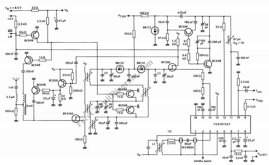
The TDA1072AT is a specialized integrated circuit designed for AM radio receivers, produced by Philips Semiconductors. This IC is intended for use in both mains-fed home receivers and car radios. It features a voltage-controlled oscillator that delivers signals with...
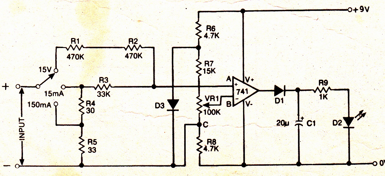
A simple electronic multimeter offers an affordable alternative for hobbyists deterred by the high cost of conventional multimeters. This device is designed to measure three ranges: (i) 0-15V, (ii) 0-15mA, and (iii) 0-150mA, with the possibility of extending the...
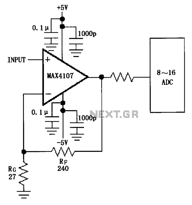
The inverting gain circuit utilizing the MAX4107 is configured as an ADC input buffer. The gain of the amplifier is established by the ratio of resistors RF and RG, which set the gain figure to approximately 10. The inverting gain...
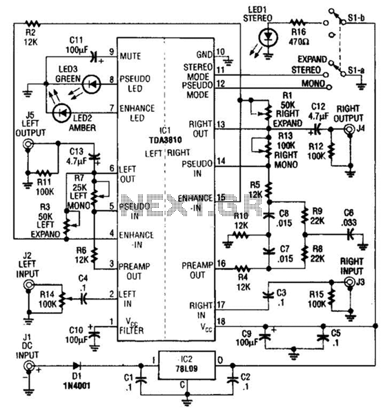
This audio processor utilizes the Signetics/Philips TDA3810N stereo, spatial, pseudo-stereo processor integrated circuit (IC). The processor employs the Philips TDA3810IC device and operates as an expander, pseudo-stereo processor, and audio enhancer. Pseudo-stereo is achieved by directing different frequencies to...

This AC to DC power supply can output 5A in continuous operation and 12A peak current. This type of DC power supply uses a PCB, allowing for two case types for IC1: TO-220 or TO-3. The regulation of this...
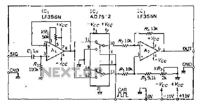
An analog switch (double loop, double-break) and a differential modulation amplifier are used in this circuit. The carrier control switch operates by switching contacts at specific times, inverting the input modulation wave. When the next carrier signal is applied...