
Analog switches carrier suppression amplitude modulation circuit

The circuit employs an analog switch configured as a double loop, double-break mechanism, which allows for precise control over the modulation process. The differential modulation amplifier serves to amplify the input modulation wave while ensuring that the signal remains within the desired amplitude limits. This configuration is critical for applications requiring high fidelity in signal transmission.
The carrier control switch is responsible for managing the timing of the modulation. It is designed to switch between different states, ensuring that the modulation wave is inverted at the appropriate intervals. This inversion is crucial for achieving the desired amplitude modulation characteristics, where the carrier signal's polarity is reversed without introducing distortion.
The circuit's operation is contingent upon maintaining a stable carrier frequency. Analog switches, while effective for low-frequency applications, are limited in their performance at high frequencies. Therefore, careful consideration must be given to the selection of components to ensure that the analog switch can handle the required frequency range without degradation of the signal quality.
The output of the modulation process is a square wave, which inherently contains high-frequency harmonics. To refine this output into a more desirable sine wave form, a band-pass filter is integrated into the circuit. This filter is tailored to allow only the desired frequency components to pass through while attenuating unwanted high-frequency noise, thereby enhancing the overall signal integrity.
In summary, this circuit design effectively combines an analog switch and a differential modulation amplifier to achieve controlled amplitude modulation. The incorporation of a band-pass filter further ensures that the output signal meets the required specifications for sine wave characteristics, making this configuration suitable for various electronic applications.Analog switch (double loop, double-break) and differential modulation amplifier complete the work. The carrier control switch, switch contacts in the time, from the inverting i nput Chi input modulation wave is inverted. Back when the next carrier-inverting input, so that the anti- re going, to achieve the limit amplitude modulation, the carrier will not braid week and intermittent, but the polarity reversal. Analog switches must keep the carrier frequency, at high frequencies can not use. The modulated output is crossing the square, containing high frequency changed as needed to increase the band-pass filter, to obtain a sine wave signal.
Related Circuits
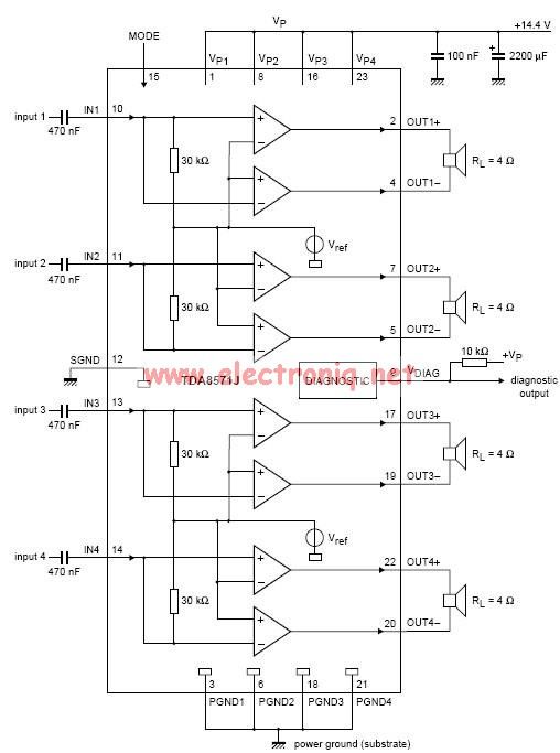
This electronic circuit diagram represents an audio power amplifier utilizing the TDA8571J integrated circuit. It is a class-B output amplifier configured in a BTL (Bridge-Tied Load) arrangement, featuring four amplifiers, each with a gain of 34 dB. The main...
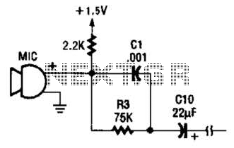
This circuit is suitable for using an electret microphone for various applications. A 1.5-V battery is utilized. CI and R3 provide treble boost and bass cut; they can be eliminated if desired. The described circuit employs an electret microphone, which...
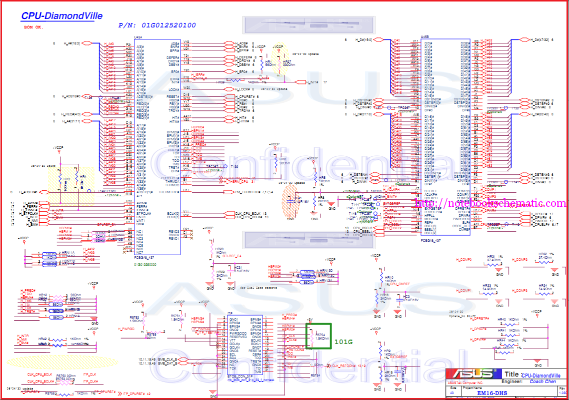
Laptop schematic circuit diagram for laptop repair and laptop BIOS password removal. The laptop schematic circuit diagram serves as a crucial resource for technicians and engineers involved in laptop repair and maintenance. This diagram provides a detailed representation of the...
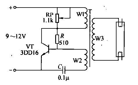
This circuit is designed for the ignition of a direct current (DC) fluorescent lamp rated between 6 to 8 watts. It utilizes a common pole-blocking oscillator that consists of a transistor (VT) and is induced by the secondary side...
Face Through attendance is the world's first embedded facial recognition machine, with an error rate of less than one in one hundred thousand and a rejection rate of less than one percent. In the field of biometrics, this device...
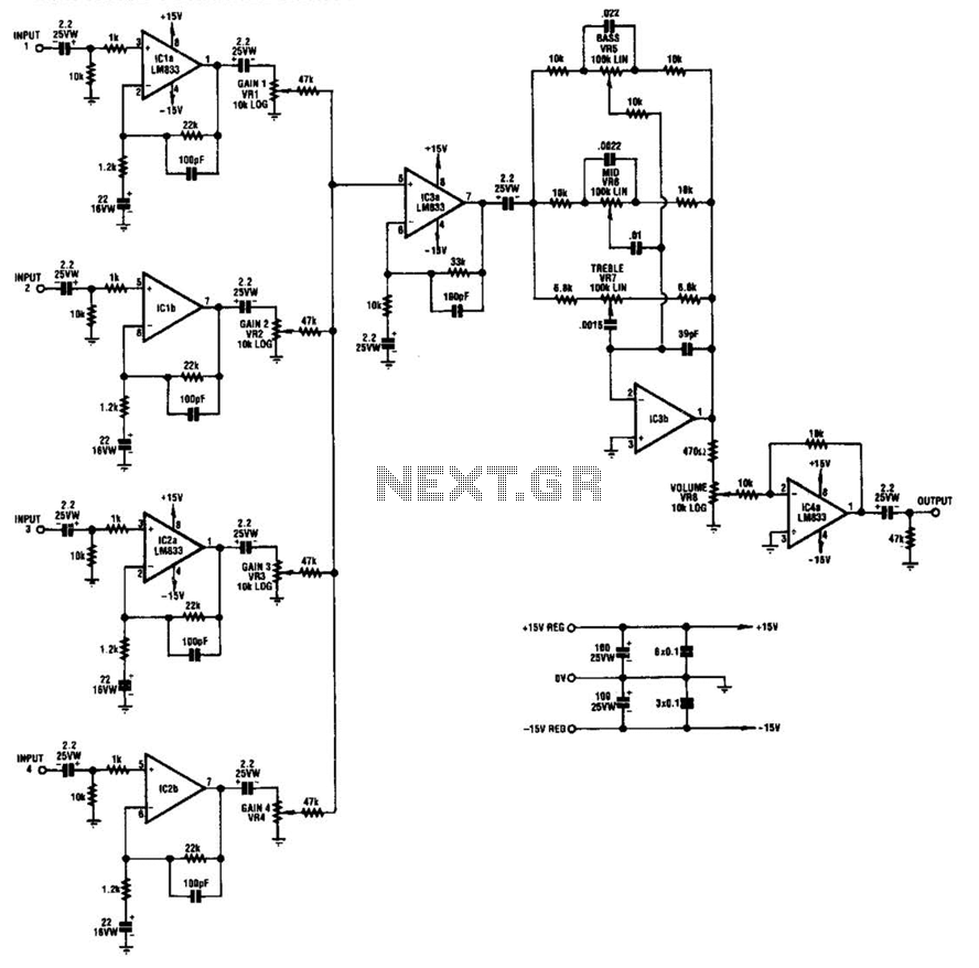
IC1-a, IC1-b, IC2-a, and IC2-b all operate with a gain of approximately 19. Their outputs are combined through level-control potentiometers, and the resulting signal is amplified by IC3-a before being sent to the tone-control stage IC3-b. Finally, the output...