
A709 a voltage follower circuit diagram

The voltage follower circuit, also known as a unity gain buffer, is characterized by its ability to provide high input impedance and low output impedance. This feature is particularly advantageous in applications where signal integrity must be maintained during transmission, as it prevents loading effects on the preceding stage. The operational amplifier's configuration allows it to replicate the input voltage at the output, ensuring that the output follows the input without amplification.
In practical applications, the voltage follower is frequently used in sensor interfaces, where the signal from a sensor must be buffered before being sent to an analog-to-digital converter (ADC) or further processing stages. The high input impedance ensures that the sensor's output is not significantly affected by the circuit's loading, preserving the accuracy of the measurement.
In the context of the operational amplifier's performance, the stability of the circuit is paramount. The presence of strong negative feedback enhances the linearity and reduces distortion, making the voltage follower suitable for high-fidelity applications. However, care must be taken to avoid conditions that could lead to instability, such as excessive input signal amplitudes that approach the power supply limits of the operational amplifier. In such cases, the circuit may enter a state of saturation, resulting in a loss of linearity and potential distortion of the output signal.
To prevent instability caused by internal oscillations, additional components such as compensating capacitors or resistors may be introduced in the feedback path. These components can help to stabilize the operational amplifier's response, ensuring consistent performance across a range of operating conditions. Additionally, selecting operational amplifiers with suitable bandwidth and slew rate specifications is critical to maintaining the desired performance characteristics in voltage follower applications.Figure (a) shows the circuit as a voltage follower, it is a special case of the in-phase amplifying circuit, the input signal from the integrated operational amplifier with the end of the introduction phase, the feedback resistor is zero, negative feedback is very strong, very stable op amp input impedance great. Output resistance is very small, so this circuit has an impedance conversion function. Impedance transformation means effect the so-called after amplifying a voltage follower, the output voltage is approximately equal to the electromotive force and the output signal source resistance is small.
The circuit is used as an input stage, an intermediate buffer stage and an output stage. The basic relationship of the circuit as follows: Vi + Vis Vo Vo -AVis Where: A-- the open-loop voltage amplification factor; Vis-- pure op amp input voltage; This circuit, when the voltage of the input signal amplitude is increased to nearly the op amps positive supply voltage, the deadlock may occur that will not be the normal output signal, which is due to the positive feedback op amp internal parasitic oscillations produced. In order to prevent this phenomenon, may be employed in Fig (b)
Related Circuits
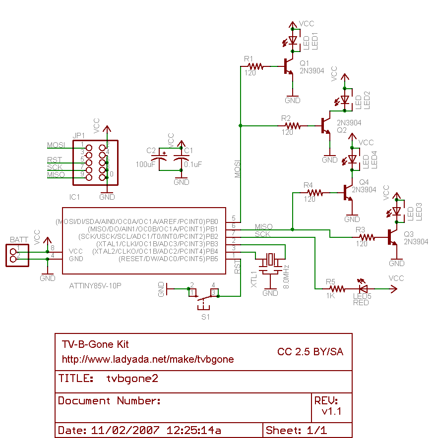
Why use one resistor and one transistor for each LED instead of connecting the LEDs in series and controlling them with a single transistor? This approach is controlled by an Arduino pin through a single resistor. While there is...
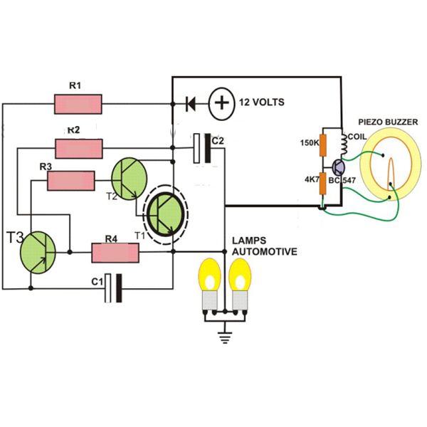
This circuit is designed to create a flasher unit for a motorbike. It is a simple turn signal flasher circuit that can be easily built and installed in any two-wheeler for the desired functionality. The circuit uses only two...
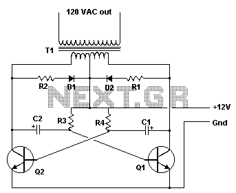
This inverter is designed to operate appliances such as TVs and stereos while traveling or camping. It converts 12 VDC to 120 VAC, with the output wattage determined by the transistors used for Q1 and Q2, as well as...
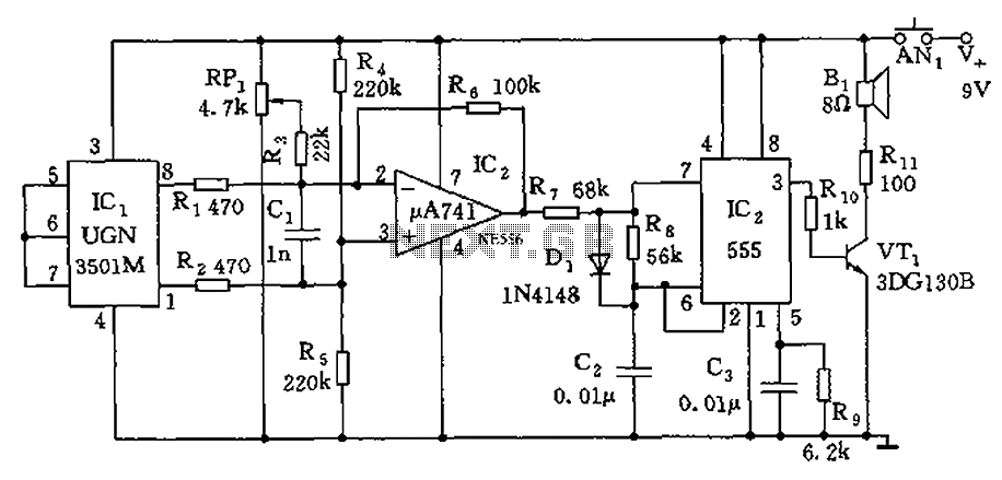
The circuit consists of a 555 timer and associated components designed for voltage-to-frequency conversion. It is utilized for determining the orientation of Earth's magnetic field using a Hall-effect sensor, specifically the UGN-3501M. This sensor incorporates a Hall element and...
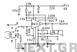
BA313 is a built-in automatic level control (ALC) circuit for audio recording preamplifiers, commonly used in cassette tape recorders. It is housed in a 9-pin dual in-line package (DIP) and features a wide range of automatic level control, operates...

The subwoofer is a speaker designed to reproduce low frequencies, specifically in the range of 20 Hz to 150 Hz. The electronic circuit diagram below illustrates the details of a subwoofer amplifier using the TDA1516, a 22-watt amplifier suitable...