
AC Millivoltmeter Adapter

The input network consists of AC coupling made of a 0.047 µF capacitor and a 10 MΩ resistor and transient protection. The -3 dB corner of the high pass filter is 0.34 Hz. Some degree of transient protection is obtained by two back-to-back emitter-base junctions, which work a lot like back-to-back Zeners. The main difference between these and Zeners is that the reverse biased junction capacitance is lower and the knee fairly sharp, meaning that it should have no measurable effect on a 200 kHz, 200 millivolt input signal.
The input of the preamp is the gate of the 2N5485 JFET, and since the drain drives the forward-biased base-emitter junction of the 2N3906, the signal on the JFET’s drain is very small, thus there is little Miller capacitance, keeping the input capacitance low.
Negative feedback through the 20 kΩ resistor from the collector of the 2N3906 and the source of the 2N5485 JFET stabilizes the DC operating point of both transistors and stabilizes the gain of the stage overall. The gain of the preamp is measured at 16X.
The 10 kΩ resistor was selected for the individual 2N5485 to set the DC level on the output of the stage. The DC level at the output is 4.7 VDC. This resistor may need to be changed for individual JFETs because of variation in the pinch-off voltage. The AC signal from the preamp is connected to a half-wave voltage doubler employing Schottky diodes. The doubler is slightly forward-biased to enhance linearity, particularly for small signals, by the voltage divider made of two 2.2 kΩ resistors and the 10 MΩ resistor. The voltage divider generates 2.5 volts on the anode of D1, while the 10 MΩ resistor provides a current return to ground from the cathode of D2.
Due to the large value of the 10 MΩ resistor, the current through the diodes is minimal, resulting in a small forward voltage drop across D1 and D2, estimated at about 250 nA. This current is typically subtracted from the input bias current of the operational amplifier, but since the input bias current of a TL062 is a couple of hundred nanoamps at room temperature, it can be neglected. The significant load of 10 MΩ and a large bias voltage source (2.5V) ensure that the current through the diode remains consistent with small signal variations, contributing to the excellent linearity of the circuit.
Testing with an oscilloscope indicates that the preamp maintains a flat response from below 1 Hz to beyond 2 MHz, with a -3 dB point. The gain remains consistent within a couple of percent past 400 kHz. If any of the semiconductors are substituted, the 50 pF peaking capacitor may require adjustment. To optimize peaking, a square wave input can be used to fine-tune the capacitor for the best square edge without visible overshoot. Any observed ringing may indicate a layout issue.Diode detectors are good at changing AC into DC, even at high frequencies. The main problem with diode detectors have inherent nonlinearities, particularly for small signals. To minimize the effects of the nonlinearities, a preamplifier boosts the amplitude of the input signal by 16X, thereby reducing the the diode detector’s nonlinearity effects by the same factor. The detector is followed by a buffer and adjustable gain stage. This last stage compensates for DC offset that results from bias on the diode detector and reduces the full scale amplitude so that the output signal DC level is equal to the input peak-to-peak value.
The input net work consists of AC coupling made of a 0.047 uf capacitor and a 10 Meg resistor and transient protection. The -3 db corner of the high pass filter is 0.34 Hz. Some degree of transient protection is obtained by two back-to-back emitter-base junctions, which work a lot like back-to-back Zeners.
The main difference between these and Zeners is that the reverse biased junction capacitance is lower and the knee fairly sharp, meaning that it should have no measurable effect on a 200 kHz, 200 millivolt input signal. The input of the preamp is the gate of the 2N5485 JFET, and since the drain drives the forward-biased base-emitter junction of the 2N3906, the signal on the JFET’s drain is very small, thus there is little miller capacitance, keeping the input capacitance low.
Negative feedback thorough the 20k resistor from the collector of the 2N3906 and the source of the 2N5485 JFET stabilizes the DC operating point of both transistors and stabilizes the gain of the stage overall. I measured the gain of the one I built at 16X. The 10K resistor was selected for the individual 2N5485 to set the DC level on the output of the stage.
On the one I built, the DC level at the output is 4.7 VDC. This resistor (10k in this schematic) may need to be changed for individual JFETs because of variation in the pinch-off voltage. The AC signal from the preamp is connected to a half-wave voltage doubler employing Schottky diodes. The doubler is just slightly forward biased to make it more linearl particularly for small singals, by the voltage divider made of 2.2k resistors and the 10 Meg resistor.
The voltage divider makes 2.5 volts on the anode of D1 and the 10 Meg resistor provides a current return to ground from the cathode of D2. Since the 10 Meg resistor is so large, the current through the diodes is very small, meaning that the forward voltage of D1 and D2 is also very small.
The current is about 250 nanoamps. From this we would normally subtract the input bias current of the of-amp, but since at room temperature the input bias current of a TL062 is a couple hundred nanoamps, it can be neglected. It should be pointed out that with the very large load of 10 Meg Ohms and a large bias voltag source (2.5V), the current through the diode will not change significantly with signal levels of a couple hundred millivolts, and I think this contributes to the excellent linearity.
Checking with an oscilloscope, the preamp appears to flat from below 1 Hz to past 2 MHz (-3 db point). It looks like the gain is flat to within a couple of percent past 400 kHz. If either of the semiconductors are substituted the 50 pf peaking capacitor may have to be changed. To check peaking, drive the input with a square wave and adjust the capacitor for the most square” edge you can get without visible overshoot.
If you see ringing, it is most likely because of a layout problem. 🔗 External reference
Related Circuits
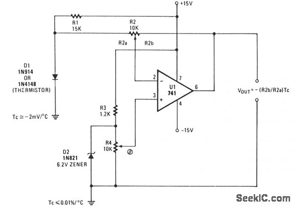
A simple operational amplifier and silicon diode form the core of a temperature-to-voltage converter, allowing the use of a standard voltmeter—either analog or digital—to measure temperature. User adjustments enable readings of either 10 mV or 100 mV to correspond...

Measures 10mV to 50Volt RMS in eight ranges. Simply connect to your Avo-meter set to 50µA range. Connect J2 and J3 to an Avo-meter set to 50µA range. Switching SW2 the four input ranges will be multiplied by 5....

The car cigarette lighter outputs a DC voltage of 12 V, which does not exceed 13.8 V even when the engine is running. A voltage of 19 V is lower than the normally required levels. The car cigarette lighter circuit...

An AC millivoltmeter - calibrated in dB - with a range of 30V down to 3mV full scale (80dB range) would be extremely useful. Attach a microphone (electret mic capsules are quite good), and you have a relative sound...
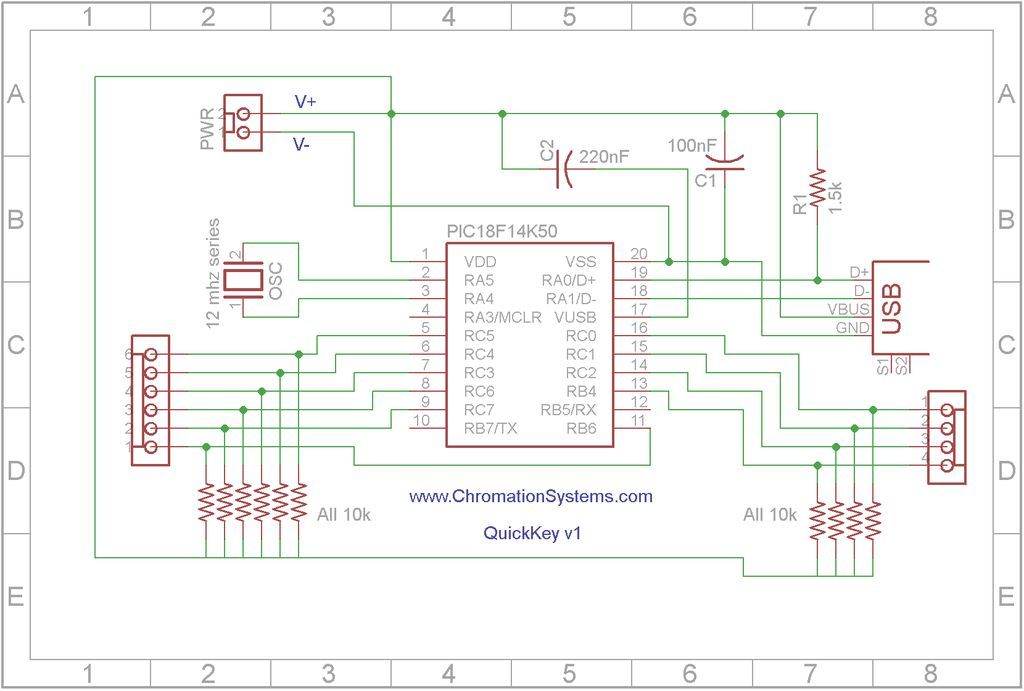
Quick Key Adapter, 10 Button HID Keyboard. This document outlines the process of creating a USB-connected Human Interface Device (HID) keyboard featuring 10 button inputs. The Quick Key Adapter is designed to facilitate user interaction through a compact keyboard interface....
Construct this circuit using any preferred method, ensuring that high voltage safety measures are strictly adhered to. Proper insulation is crucial, and bare conductors must be spaced at least 2mm apart to avoid arcing. This circuit functions as a...