
ADIADM106610 a power monitors and sequencing control solution

The ADM106x Evaluation Board is designed to demonstrate the device's features in a compact and self-contained environment. It includes a simple block diagram illustrating the board's functions, detailed schematics, and the tracking, power, and silkscreen layers. The evaluation board features eight programmable voltage circuits labeled VX1 to VX4 and VP1 to VP4, which can be programmed via software over a voltage range of 0.6V to 6V. These circuits supply voltages to eight of the ten inputs of the ADM106x, with VX5 serving as a test point for user-defined external input and VH receiving a direct 12V supply or an optional programmable supply from VP4. The board also features ten output indicator LEDs labeled PDO1 to PDO10, which indicate logic high on the output pins of the ADM106x. LEDs PDO1-6 are dual-color, signaling whether a PDO is functioning as a logic output (green) or as a FET driver output (red).
The main evaluation board contains all necessary circuitry to actively stimulate the ADM1062-69 devices and monitor their responses, including programmable supplies, ADCs, and LEDs. A daughter-card socket is provided for compatibility with different packaging options (LFCSP, TQFP, or LQFP), allowing for the use of specific devices in conjunction with the main evaluation board. Device samples are included in a sample box, and a single device should be placed in the socket prior to powering the evaluation board. Connectivity to a PC is facilitated through an SMBus cable for a parallel connector or a USB cable for a USB port, with power supplied separately or through the PC USB, respectively.The ADI Company one ADM1066 is it monitor one piece powers many kinds of of configurated /sequence device, and last 12 ADC and 6 8 DAC of voltage output, all voltage is superior to 0. 5% in the precision of 25 degrees of C, is mainly used in the office system of the centre, server / router, the systematic circuit card of many voltage, sequence of DS
P/FPGA voltage, etc. This text has introduced ADM1066 key feature, the block-diagram, employs block diagram and ADM106x Evaluation Board key feature, block-diagram and circuit diagram, material bill. The ADM1066 Super Sequencer is a configurable supervisory/ sequencing device that offers a single-chip solution for supply monito ring and sequencing in multiple-supply systems.
In addition to these functions, the ADM1066 integrates a 12-bit ADC and six 8-bit voltage output DACs. These circuits can be used to implement a closed-loop margining system that enables supply adjustment by altering either the feedback node or reference of a dc-to-dc converter using the DAC outputs.
Supply margining can be performed with a minimum of external components. The margining loop can be used for in-circuit testing of a board during production for example, to verify board func-tionality at 5% of nominal supplies, or it can be used dynamically to accurately control the output voltage of a dc-to-dc converter. The ADM106x Evaluation Board is designed to provide all of the necessary stimuli to the ADM106x, showing the many features of the device in a compact, self contained environment.
The following pages contain a simple block diagram of the functions on the board, followed by a detailed schematic of the board and finally, the tracking, power and silkscreen layers for board. The two main features of the board are the programmable voltage circuits and the output indicator LED` s.
There are eight programmable voltage circuits provided. The circuits are labeled VX1, VX2, VX3, VX4, VP1, VP2, VP3, VP4. These are programmable, via the Eval Board software, over a voltage range of 0. 6V to 6V. Programming of these supplies is detailed in the software section of this Eval Note. The eight circuits provide voltages to eight of the ten inputs to the ADM106x. The inputs which do not have a programmable supply are VX5 where a test point is available for the user for their own external input and VH, which has 12V driving it directly or alternatively, uses the programmable supply of VP4, if required. The ten output indicator LED` s are labeled PDO1 to PDO10. These indicate a logic high on the output pins of the ADM106x. The LED` s for PDO1- 6 are dual colour LED` s. This is to indicate when a PDO is being used as a logic output or as a FET driver output. Green indicates a logic output while red indicates a FET driver output. Main Evaluation Board: This board contains all of the circuitry necessary to active stimulate the ADM1062-69 devices and mon itor its response, such as programmable supplies, ADCs, LEDs, etc.
Daughter-card Socket: A relevant daughter-card with a device socket is also supplied. There are three different daughter-card options for the main evaluation board depending on the packag e option-LFCSP, TQFP or LQFP. The daughter-card plugs directly into the main evaluation board and allows all the devices in their s pecific layouts to be used in conjunction with the main evaluation board.
The correct one will be supplied for the devices included in the kit. Device Samples: Some loose samples of the device to be evaluated are included in a samples box. A single device should be placed in the socket before powering up the evaluation board. SMBus Cable: This cable connects the main evaluation board to a standard PC parallel connector. Power must be applied to the board separately if using this cable. USB Cable: This cable connects the main evaluation board to a standard PC USB port. Power for the evaluation board will also be provided by the PC USB 🔗 External reference
Related Circuits
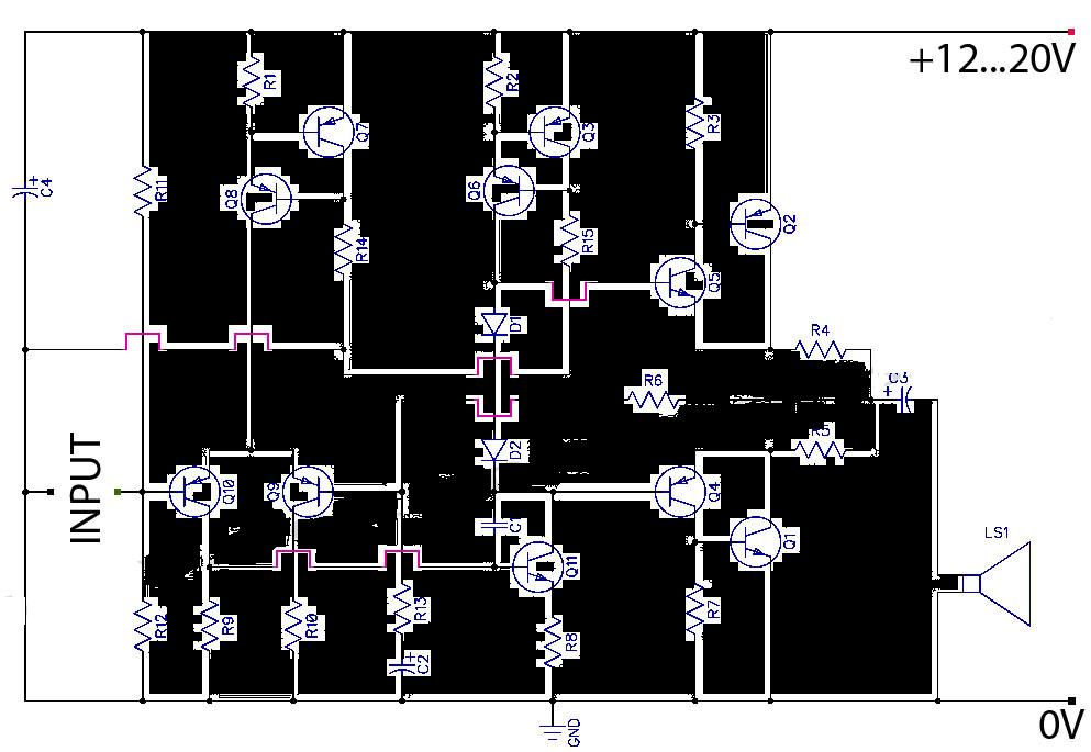
This is a Class AB transistor power amplifier. It is straightforward to construct, utilizing standard components, and is known for its stability and reliability. The entire circuit employs commonly available parts and can be easily assembled on a general-purpose...

The schematic of the power supply is illustrated below. It operates using standard household power of 120VAC at a frequency of 50/60Hz, with an adjustable output that can reach up to 25kV or higher. The power supply circuit is designed...
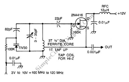
A voltage-controlled oscillator (VCO) is an electronic signal generator that produces a signal with a variable frequency, which is dependent on an input voltage level. A voltage-controlled oscillator is a fundamental component in various electronic applications, including phase-locked loops (PLLs),...
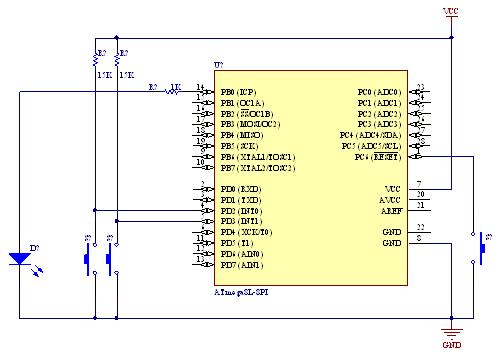
A demonstration of external interrupts in the AVR (Atmega8) microcontroller, including a circuit diagram and C code for the interrupt service routine (ISR). The Atmega8 microcontroller is a versatile device widely used in embedded systems, particularly for applications requiring external...
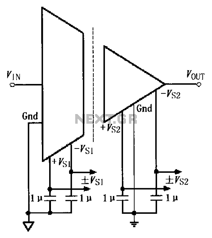
The basic connection circuit for the ISO122/124 includes power and signal connections. Each supply terminal of the ISO122/124 must be equipped with a 1 µF tantalum capacitor serving as a bypass filter. It is important to position the printed...
When a key is pressed, the remote control transmits a preamble followed by 32 bits of information encoded using specific pulse timings. The pulse examples can be observed in logic analyzer screen captures, although some glitches are present due...