
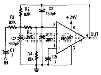
Adjustable notch filter

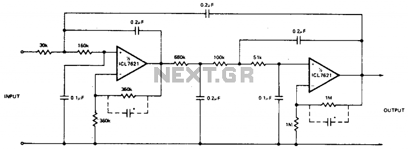
A secondary voltage follower is required to drive the twin "T" network from a low-resistance source, ensuring that neither the notch frequency nor the depth is affected by the settings of the potentiometer.
In this circuit design, the notch filter is implemented using a twin "T" configuration, which is known for its effectiveness in rejecting specific frequencies while allowing others to pass. The Q factor, an indicator of the selectivity or sharpness of the notch, can be finely tuned between 0.3 and 50, allowing for flexibility in various applications. A lower Q factor results in a broader bandwidth for frequency rejection, which can be particularly useful in environments where signals may vary.
The use of a secondary voltage follower plays a crucial role in maintaining the integrity of the notch filter's performance. By providing a low-resistance source, it ensures that the feedback mechanism does not alter the desired notch characteristics as the potentiometer is adjusted. This feedback loop, which incorporates components R3 and C3, is essential for controlling the notch Q. The amount of signal fed back into the circuit directly influences the filter's performance, allowing for precise adjustments to meet specific application requirements.
Overall, this circuit demonstrates a sophisticated approach to frequency filtering, combining adjustable Q factors with robust feedback mechanisms to achieve reliable and consistent performance across a range of input conditions. The design is particularly suitable for applications in audio processing, communication systems, and any scenario where precise frequency rejection is necessary.In applications where the rejected signal might deviate slightly from the null on the notch network, it is advantageous to lower the Q of the network. This insures some rejection over a wider range of input frequencies. The figure shows a circuit where the Q may be varied from 0.3 to 50. A fraction of the output is fed back to R3 and C3 by a second voltage follower, and the notch Q is dependent on the amount of signal fed back.
A second follower is necessary to drive the twin "T" from a low-resistance source so that the notch frequency and depth will not change with the potentiometer setting.
Related Circuits
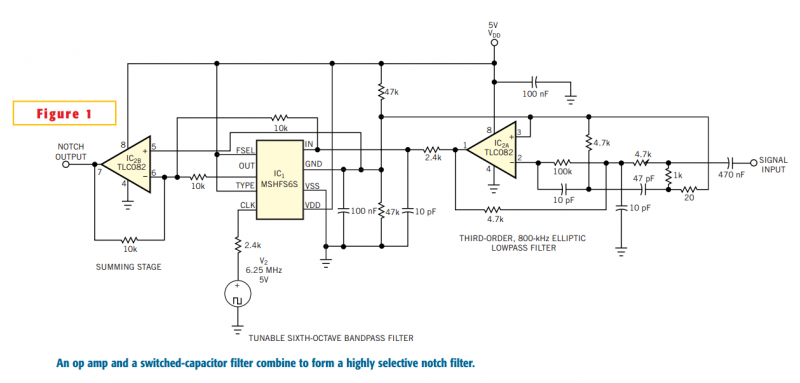
Although you can obtain universal, resistor-programmable switched-capacitor filters that are configurable as notch filters, most cannot operate at bandwidths higher than 100 kHz. Further, the typically 16- to 20-pin packages do not include a continuous-time, antialiasing filter to prevent...
Designed to produce a 12-dB/octave roll-off above the 10-kHz cutoff frequency, this low-pass active filter will help reduce needle scratch on records. It utilizes an LM387 low-noise amplifier integrated circuit (IC). The low-pass active filter described is engineered to attenuate...
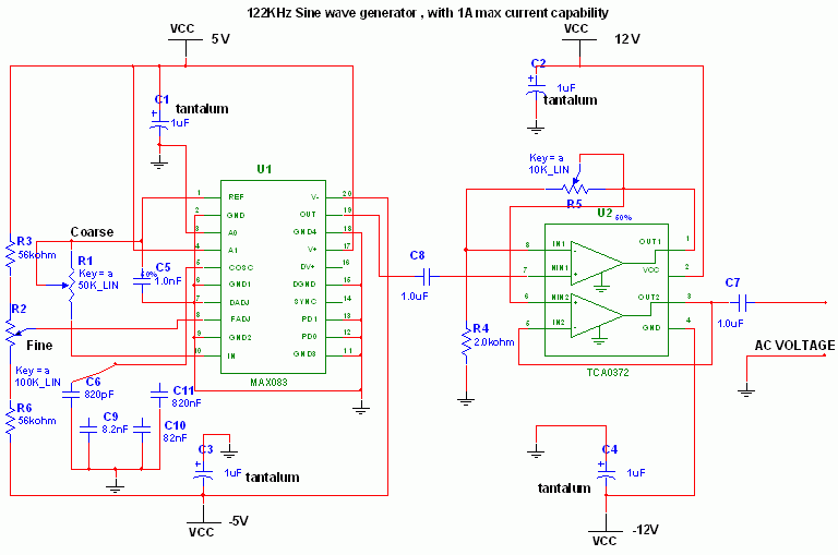
This circuit utilizes the versatile MAX038 function generator. While some advanced features of this integrated circuit (IC) are disabled in this configuration, it is capable of generating sine, triangle, and square waves by adjusting the A0 and A1 pins,...
This project involves the design of an air-filter sensor intended for use in home heating and cooling systems. The project encompasses conceptual design, analysis, implementation, testing, and modifications. Initially, the study focuses on comparing air quality and power consumption...
The hum noise is produced by an electronic device with improper design. To address this issue, it is essential to identify the source of the hum. This involves checking the grounding, cabling, casing, and other factors that may contribute...
The low bias currents allow for the utilization of high resistance and low capacitance values, facilitating a low frequency cutoff at fc = 10 Hz, with an AVCL of 4 and a passband ripple of 0.1 dB. Additionally, small...