
Atv Downconverter Circuit

The RF converter is designed to facilitate the reception of amateur television signals within the specified frequency range of 420 to 450 MHz by converting these signals to VHF channels 3 or 4. This conversion enables standard television receivers to process and display the amateur TV signals effectively.
The circuit architecture includes several critical components. The RF amplifier (Q1) serves to boost the incoming RF signals before they are fed into the mixer (M1). The mixer is essential for down-converting the frequency of the RF signals to an intermediate frequency (IF) that can be further processed. The output of the mixer is then amplified by the IF amplifier (Q3), which ensures that the signal remains strong enough for subsequent stages of processing.
An important feature of this RF converter is the oscillator (Q2), which operates around 378 MHz. This oscillator is tunable over a range of approximately 30 MHz, allowing for flexibility in the conversion process. The tuning capability is crucial for accommodating variations in the incoming signal frequencies, ensuring optimal performance and signal clarity.
Overall, this RF converter circuit is an effective solution for receiving amateur TV signals, utilizing a combination of amplification, mixing, and tuning to provide a reliable output compatible with standard television equipment. This RF converter converts amateur TV signals in the 420- to 450-MHz region to VHF channel 3 or 4, allowing reception of those signals on a standard TV receiver. RF amplifier Ql feeds mixer Ml, and Q3 acts as an IF amplifier. Q2 is an oscillator operating around 378 MHz and is tuneable over about a 30-MHz range.
Related Circuits

Emits a beep if the door remains open for more than 20 seconds. This circuit is housed in a compact enclosure and is positioned in the refrigerator near the lamp or the opening. The described circuit functions as a door...
This simple circuit can be used to charge a pair of AA or AAA-sized cells using solar energy. It has been utilized to maintain the operation of devices such as a Palm Pilot and a Walkman radio continuously. This...
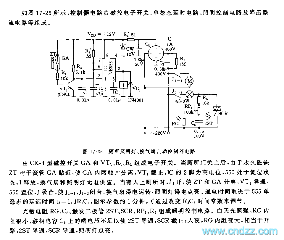
The electronic switch consists of the CK-4 type magnetic control switch and the components VT1, R1, and R2. When the bathroom door is closed, the permanent magnet ZT and the reed switch GA come into proximity, which separates the...
The circuit is designed for sound and light control of stairway and walkway lighting. It features high immunity and includes soft-start and over-current protection mechanisms. During the day, the photosensitive resistor has low resistance, resulting in a low voltage...

This universal battery charger utilizes the LM317 voltage regulator and features an adjustable output voltage along with a constant-current charging circuit, making it suitable for charging most NiCad batteries and various other battery types. The LM317 universal battery charger...
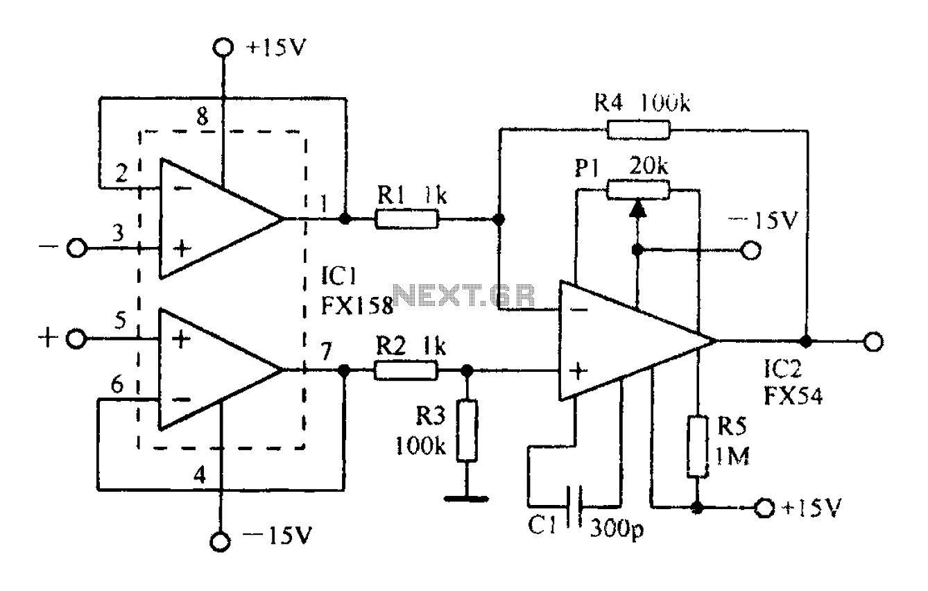
A differential amplifier with input impedance as indicated in the circuit diagram. A differential amplifier is a crucial component in various electronic applications, primarily used to amplify the difference between two input voltages while rejecting any common-mode signals. This characteristic...