
Basic Flash Memory Programming Voltage Supply

The basic flash memory programming voltage supply circuit is designed to provide the necessary high voltage for programming flash memory devices. The core component of this circuit is the LT1072, a high-efficiency switching regulator that is capable of stepping up low input voltages to higher levels required for programming operations.
In this configuration, the LT1072 operates in a boost converter mode. When the circuit is powered on, the LT1072 begins to switch on and off rapidly, controlling the current flow through the inductor L1. As the inductor stores energy during the "on" phase, it generates a magnetic field. When the LT1072 switches to the "off" phase, the magnetic field collapses, and the energy stored in the inductor is released. This energy transfer results in a higher voltage output, which is essential for the flash memory programming process.
Resistor R2 plays a crucial role in regulating the output voltage level. By selecting an appropriate resistance value, R2 helps to determine the output voltage that will be delivered to the flash memory device. This output voltage needs to be carefully controlled to prevent damage to the memory components while ensuring reliable programming.
Additional components may include input and output capacitors to stabilize the voltage levels and filter out any noise that could affect the performance of the circuit. A diode may also be included in the circuit to prevent reverse current flow, which could potentially damage the LT1072 or other components in the circuit.
Overall, this flash memory programming voltage supply circuit is a vital tool for applications requiring high voltage for programming flash memory devices, ensuring efficient and safe operation during the programming process.This is a Basic Flash Memory Programming Voltage Supply circuit. This circuit uses LT1072 switching regulator to generate high voltage by driving the L1. R2 and. 🔗 External reference
Related Circuits
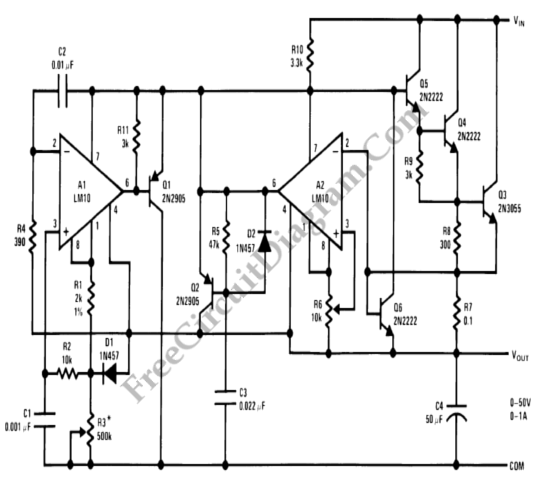
A laboratory power supply is characterized by its wide adjustable voltage range and robustness. Continuous voltage adjustment is necessary, as well as a current limiter for safety and reliability. A suitable design can be created using the LM10 operational...
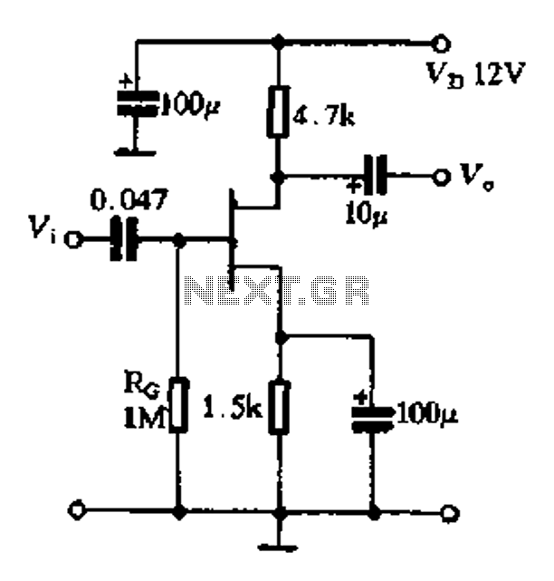
The FET exhibits a high input impedance, a low noise figure, anti-crosstalk capabilities, and good mutual interference performance, making it increasingly utilized in electronic circuits. FET amplifiers can be configured in various ways, including as common source (equivalent to...

Common emitter amplifier circuit with resistance and capacitance coupling. The common emitter amplifier circuit is a fundamental configuration in analog electronics, widely utilized for its ability to amplify voltage signals. This circuit employs a bipolar junction transistor (BJT) as the...
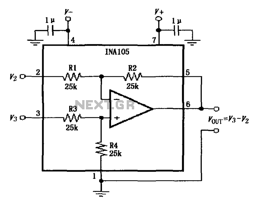
The power supply terminal should utilize a 1 µF chip capacitor filter, positioned as close as possible to the chip's supply pin. The signal is generated by the input pins 2 and 3. The source resistance of the signal...
A switching power supply with an output voltage significantly lower than its input voltage exhibits an interesting characteristic: the current drawn by the supply is less than its output current. However, the input power (UI) is greater than the...
This low-voltage, high-current output switching power supply operates from a 220 VAC input. In this circuit, an ST2 diac relaxation oscillator, along with Q3, C1, and the diac, initiates the conduction of the output switching transistor Q1. The on-time...