
Basic Logic Gate with PNP Transistor

The described circuit employs PNP transistors to create a versatile logic gate configuration. In digital electronics, logic gates are fundamental building blocks used to perform logical operations on one or more binary inputs to produce a single binary output.
In this specific schematic, the PNP transistor can be configured to operate as an OR gate when the inputs are connected in such a way that if either input is activated (i.e., brought to a low state), the output will also be activated (high state). Conversely, when configured as an AND gate, the circuit will only output a high state when both inputs are in a low state.
The operation of the PNP transistor is based on the principle that it conducts when the base is at a lower potential than the emitter. Therefore, the arrangement of resistors and the connections to the inputs are critical to achieving the desired logical functionality.
The transistor's biasing must be carefully considered to ensure that the desired logic levels are correctly interpreted. Resistors may be used to limit the current flowing into the base of the transistor and to establish the necessary voltage levels for proper operation.
In practical applications, this circuit can be utilized in various digital systems, including simple calculators, alarm systems, and other devices requiring basic logical decision-making capabilities. The simplicity of the PNP transistor circuit allows for easy integration into larger systems while providing reliable performance.
Overall, this schematic serves as a foundational example of how PNP transistors can be employed in digital logic design, showcasing their versatility and importance in electronic circuit design.This schematic diagram shows a circuit of basic logic gate circuit. This PNP transistor circuit can act as OR gate or AND gate. If the input is closing of. 🔗 External reference
Related Circuits
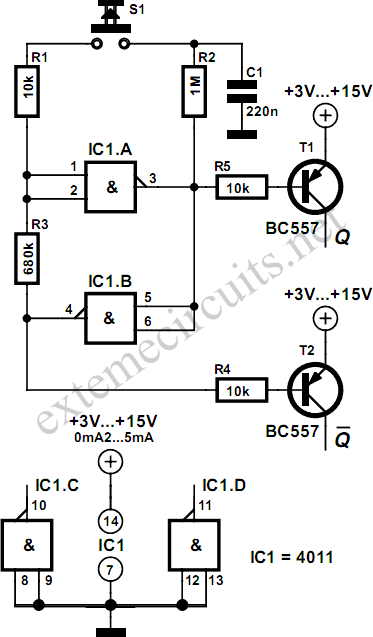
Using just two NAND or inverter gates, it is possible to build a D-type (or toggle) flip-flop with a push-button input. At power-up, the output of gate N2 is at a logical 1, ensuring that transistor T2 is switched...
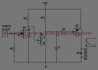
This document describes a series of touch switches that utilize only three transistors. These touch-based transistor switches can activate a load simply by the user touching a metal plate. They are designed to directly switch a relay, enabling operation...
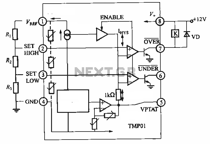
TMP01 is a temperature sensor that features a programmable temperature controller, an integrated reference voltage source, a current source, a voltage comparator, and an amplifier circuit. The internal circuit function block diagram and basic application circuit are provided. The key...
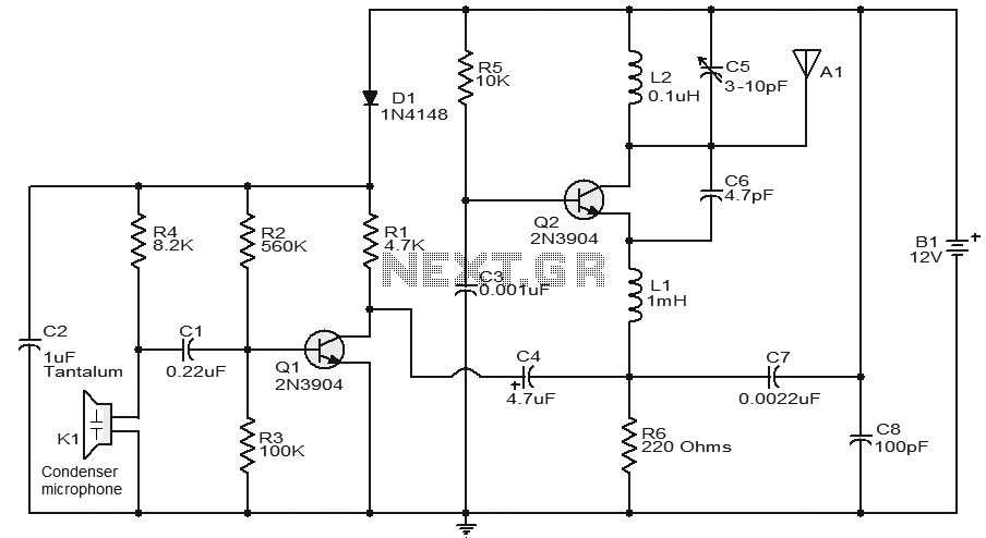
This circuit features a very stable and simple FM transmitter design. This transmitter can achieve a range of approximately 200 meters when properly matched. The FM transmitter circuit typically consists of several key components: an oscillator, modulator, amplifier, and antenna....
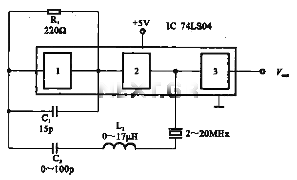
The circuit includes several gates arranged as a crystal oscillator circuit. Figure (A) illustrates a crystal oscillator circuit operating at 1 MHz, while Figure (B) depicts a 20 MHz crystal oscillator circuit. Figure (C) represents a variable crystal oscillator...
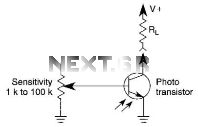
A variable resistor is utilized to adjust the light-level response of a phototransistor. Phototransistors exhibit higher light sensitivity compared to photodiodes; however, they typically demonstrate a lower frequency response. A variable resistor, often referred to as a potentiometer or rheostat,...