
bias current compensation circuit

The bias current compensation circuit is designed to mitigate the effects of input bias currents in operational amplifiers, particularly in precision applications. The LM11 operational amplifier, known for its low offset voltage and bias current characteristics, serves as the core component of this design. The circuit aims to maintain a balanced input condition, which is crucial for minimizing offset errors that can affect the accuracy of signal processing.
In the context of this circuit, the operational amplifier's two inputs are subjected to source resistances that can introduce offset voltage variations. By employing a bias current compensation scheme, the circuit effectively reduces the impact of these resistances. The design ensures that the bias currents flowing into each input are equalized, thus preserving the integrity of the output signal.
For applications such as integrators and sample-and-hold circuits where maintaining precise voltage levels is critical, the challenge lies in achieving equal resistance at both inputs without compromising the circuit's functionality. In these instances, alternative methods may be required to further reduce bias current effects, such as utilizing additional components or selecting operational amplifiers with even lower bias current specifications.
Overall, this bias current compensation circuit represents a valuable approach for enhancing the performance of analog signal processing systems, particularly in scenarios where offset voltage precision is essential. The careful selection of components and design configurations can lead to significant improvements in circuit accuracy, making it suitable for a wide range of electronic applications.This is design circuit of bias current compensation circuit. This circuit can operate from MW source resistances with little increase in the equivalent offset voltage. This circuit is based on LM11. This is the figure of the circuit. This is impressive considering the low initial offset voltage. The situation is much improved if the design can be configured so that the op amp sees equal resistance on the two inputs. However, this cannot be done with all circuits. Examples are integrators, sample and holds, logarithmic converters and signal-conditioning amplifiers. And even though the LM11 bias current is low, there will be those applications where it needs to be lower.
🔗 External reference
Related Circuits
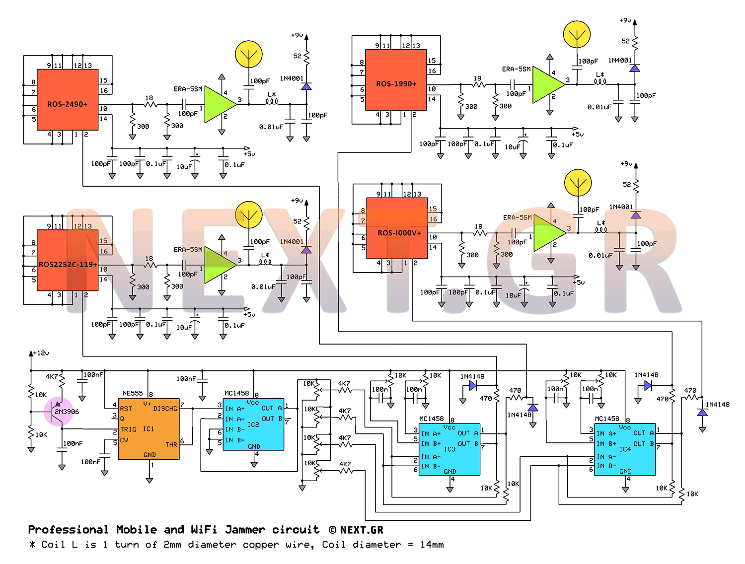
This jammer circuit can be utilized both indoors and outdoors, providing a coverage range of approximately 30 meters to disconnect wireless devices from their communication with the base station. The circuit design employs frequency ranges allocated to mobile operators,...

RS232 to RS485 Converter Circuit Schematic. RS232 to RS485 converters are primarily utilized in industrial and commercial settings. The RS232 to RS485 converter circuit is designed to facilitate communication between devices using different serial communication standards. RS232 is commonly found...
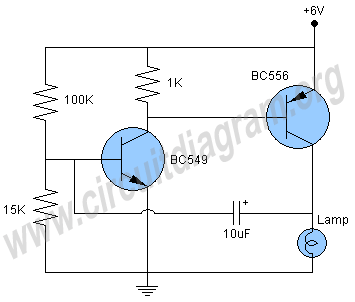
This is a simple two-transistor lamp flasher circuit that can be used to flash a 6-volt lamp. The circuit is compact and can be easily fitted into a small enclosure. It utilizes two transistors: one is an NPN BC549,...
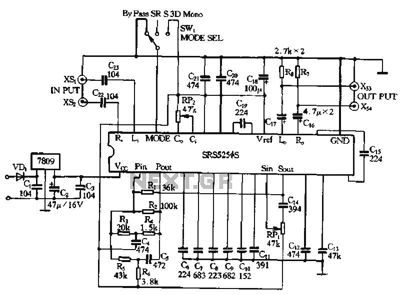
Typical application circuits for the Zheng brick SRS5250S are illustrated in the provided diagram. The SRS5250S features a pin diagram and a processing circuit that allows the user to switch between three operating modes: straight, SRS, and single-channel analog...
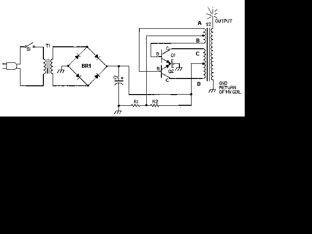
This circuit is designed to demonstrate high frequency and high voltage, capable of producing approximately 30kV, depending on the transformer utilized. It is cost-effective and straightforward to construct, primarily using a standard TV flyback transformer. This circuit can power...
Used as a 10-second momentary illuminator, this circuit can be useful in other applications as well. Pressing SI charges CI, which holds Q1 on and keeps the LED lit for about 10 seconds. The circuit described functions as a momentary...