
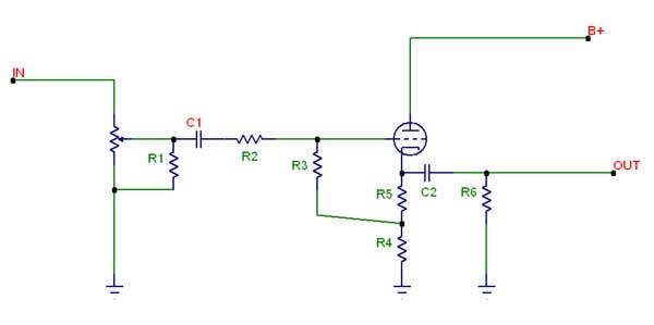
Blochead Diamond Buffer

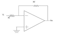
The described circuit employs a 100k volume potentiometer, serving as the input stage for either line-level signals or headphone outputs. The non-inverting gain stage provides an amplification of 15 dB, which is suitable for boosting low-level audio signals to a more manageable level before further processing. This gain stage is critical in ensuring that the subsequent buffer stage receives a strong enough signal to maintain fidelity and performance.
The buffer stage, based on a discrete configuration of the LH0002, utilizes four transistors that are meticulously matched. This matching is essential for ensuring low output offset voltage, which is crucial in audio applications where even minor voltage offsets can lead to audible distortion or imbalance in sound reproduction. The design's decision to avoid including the buffer in the feedback loop of the operational amplifier is a notable aspect, as it allows for a more straightforward circuit design while still achieving desired performance metrics.
However, the buffer's architecture presents certain inefficiencies. The need for the driver transistors to draw the same amount of current as the output devices leads to a significant increase in overall current consumption—about three times that of a more conventional design. This elevated current demand can be a drawback in terms of power efficiency, particularly in battery-operated applications.
The use of very small damping resistors on the output emitters is a critical design consideration. These resistors serve to stabilize the output stage and maintain linearity. If the resistors are too large, the output stage may not pull static current effectively, leading to a transition to Class B operation, which can introduce distortion and reduce sound quality. The minimalist approach taken in this design emphasizes simplicity and efficiency, aiming to deliver high-quality audio performance while minimizing components and complexity.
Overall, this circuit exemplifies a thoughtful balance between performance and simplicity, making it suitable for both line-level and headphone applications while addressing key challenges in audio amplification design.The circuit is designed to run off a 100k volume pot, and be either a line stage or a headphone amplifier. It is a standard non-inverting gain stage (A=15dB) followed by discrete copy of the old LH0002 buffer IC.
The basic idea is that the four transistors in the buffer will be carefully matched to ensure low output offset voltages and low distortion, so that it will not be necessary to include it in the op amp feedback loop. The rather primitive buffer is inefficient as the driver transistors must pull as much current as the output devices, so the total current is about 3x more. It also means the damping resistors on the output emitters can only be very tiny otherwise the output stage pulls no static current and reverts to class B operation.
I am drawn to the minimalist design however. 🔗 External reference
Related Circuits
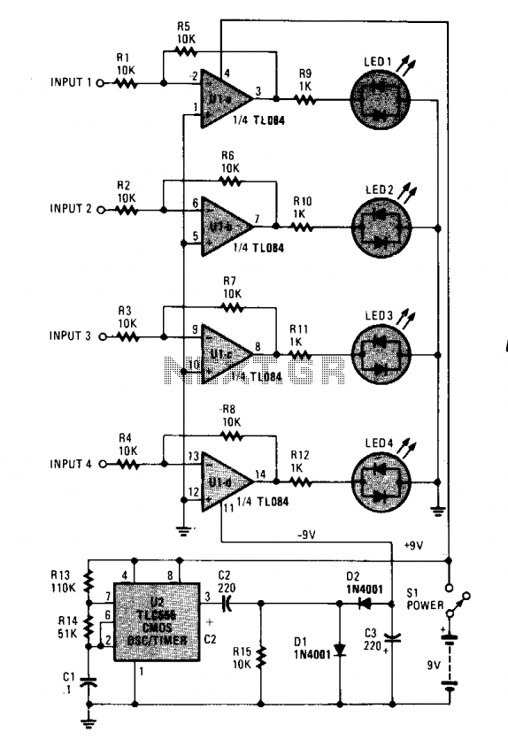
The monitoring circuit consists of four tri-color LEDs driven by an equal number of operational amplifiers configured as inverting amplifiers with a gain of one. Each LED is wired such that it illuminates red when the input to the...
The series consists of input buffers that match the output. This configuration resembles a common collector circuit with a reinforcement factor of 1. A resistor value is included to limit the current usage. The effectiveness of this circuit largely...
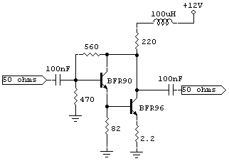
A 3KHz-50MHz signal generator is available, and there is a requirement to amplify its 2.3mW output to +7dBm. The need is for a broadband amplifier capable of achieving this amplification. To amplify the output of a signal generator from 2.3mW...
Almost all DC amplifier circuits are utilized as the input stage of differential circuits. Many complementary symmetry circuits also employ a double differential complementary sub-circuit along with a constant current source for the input stage. The constant current source...
By sufficiently lowering the output impedance of a circuit and supplying enough current to drive cables, it avoids the issues faced by passive designs. This approach seems to address many of the inherent problems in both active and passive...
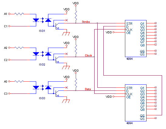
This circuit connects to a single parallel port, enabling control of electronic circuits that require up to 96 digital outputs with optically isolated lines, powered by 3 to 15V. The CD4094B is an 8-bit shift register combined with an...