
CD4001 composed of single-channel modulator

The circuit described utilizes the CD4001 IC, which consists of four independent NOR gates, making it suitable for various digital logic applications. In this configuration, two of the NOR gates are utilized to create a multivibrator, which generates a square wave signal. The oscillation frequency of 40 kHz is primarily determined by the external components, specifically the resistor R3 and capacitor C1. By altering these component values, the frequency can be adjusted, allowing for flexibility in the application.
The control mechanism is implemented via switch S1, which functions as a manual input to the circuit. When S1 is pressed, it sends a low signal to the input of NOR gate IC1-1, triggering the oscillation. This feature is particularly useful for remote control applications, where the ability to start and stop the transmission is critical.
The output from the multivibrator stage is a square wave with a 50% duty cycle, which is ideal for modulation purposes. The subsequent NOR gates, IC1-3 and IC1-4, serve as a buffer stage, providing increased drive capability to ensure that the output signal can effectively drive the next stage of the transmission circuit without distortion or degradation.
Overall, this circuit exemplifies a straightforward yet effective design for generating modulated signals for remote control applications, leveraging the properties of the CD4001 NOR gate IC to achieve reliable performance with minimal components.Core elements of this circuit is the second four-input NOR gate terminal IC CD4001, the entire circuit is simple structure, less components, easy to make, especially for remote control transmitter or a carrier modulation transmission. As shown in the specific circuit-channel remote control transmitter modulator NOR gate IC1-1, IC1-2 composition multivibrator, the oscillation frequency is 40kHz. On input NOR gate IC1-1 for control terminal, when it is high, the circuit stop vibration; when it is low, start-up circuit.
Switch Sl to the control button when Sl is pressed, the input terminal of the NOR gate IC1-1 is low, the oscillator circuit to work, the output 40kHz, 50% duty cycle of continuous square wave. Change in resistance or capacitance Cl R3 can change the oscillation frequency of the circuit. NOR gate ICl-3, ICl-4 composition of the buffer stage for improving circuit drive capability. The modulator output signal sent to the subsequent transmission circuit.
Related Circuits
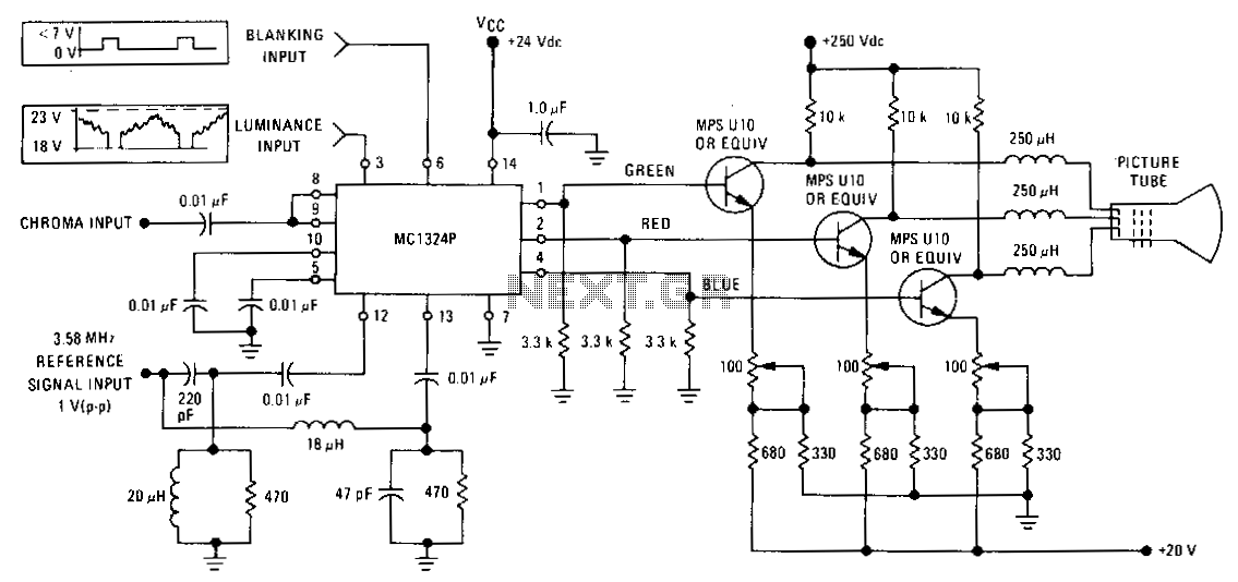
The MC1324 provides chroma demodulation, recovering the R, G, and B signals to drive video amplifiers for each color difference signal. The luminance signal and chrominance signal are matrixed to obtain the R, G, and B signals. The MC1324 is...
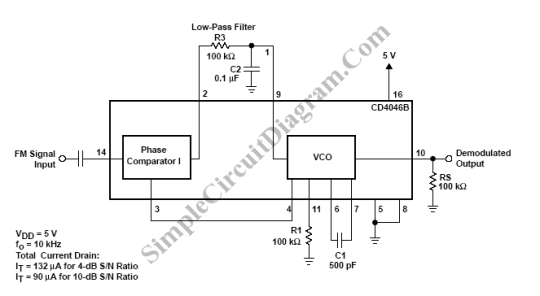
A Phase Locked Loop (PLL) can be utilized to create a Frequency Modulation (FM) demodulator. The PLL circuit tracks the input frequency by adjusting the voltage input of a Voltage-Controlled Oscillator (VCO). The Phase Locked Loop (PLL) is a critical...
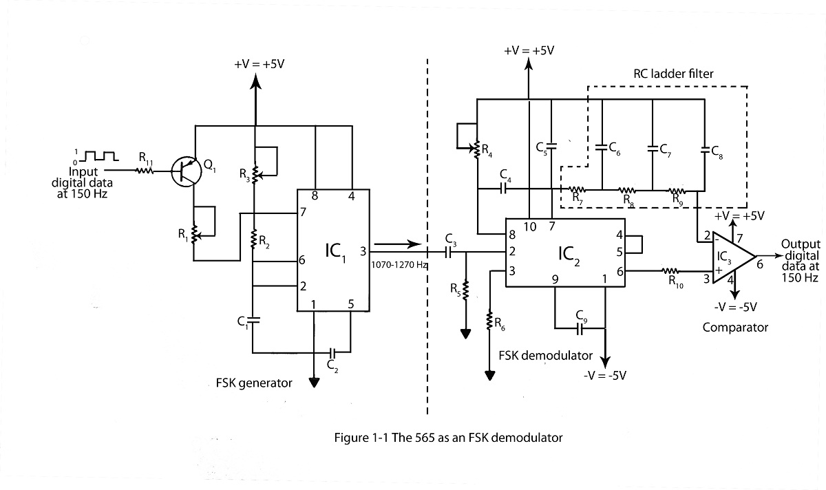
The frequency shifting keying technique is utilized to transmit binary data. The circuit diagram includes a description of an FSK demodulator that employs the 565 integrated circuit for frequency shift keying. The frequency shift keying (FSK) technique is a form...
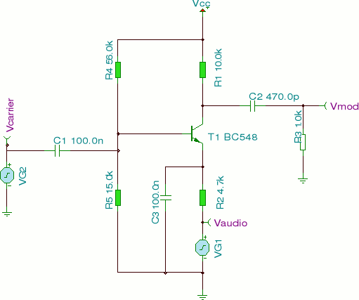
This circuit employs two signal generators to simulate an amplitude-modulated RF carrier wave. The output can be utilized to analyze the response of LC and tank circuits. One signal generator represents a high-frequency RF carrier at 200 kHz (VG2),...
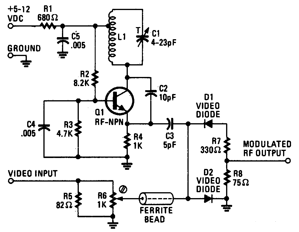
The VHF frequency is generated by a tuned Hartley oscillator circuit. Resistors R2, R3, and R4 bias the transistor, with a tapped inductor L1 and a trimmer capacitor C1 forming the tank circuit. Adjusting C1 determines the frequency. Capacitor...

The circuit illustrated in the figure depicts an automatic bathroom light switch system. When the door is opened, the light is activated, illuminating the space. Conversely, when the door is opened again, the light turns off. The circuit comprises...