
Circuit examples

The circuit can be used for CV or audio applications. The number of inputs and outputs can be increased to the desired value of columns and rows. For each of the outputs the two OpAmp circuit with the corresponding output socket is required. For each input another socket and the corresponding quantity of potentiometers and resistors is required. To obtain a higher or smaller overall amplification the feedback resistor of the first (left) OpAmp of each output circuits has to be adjusted (as described above).
The left picture shows the basic circuit of a manual gate. The 470 Ohm resistor serves as a short circuit protector. Without this resistor the +12V supply would be shorted to GND if a patch cable is inserted to the socket while the button is pressed. The left picture shows the circuit of "or-wired" sockets. This circuit is useful to combine gate or trigger signals. The incoming signals are or-wired, i. e. if any of the inputs is "high" the output turns "high" too ("high" means a positive voltage in the range of typical +5.
+12V). If none of the inputs is high the 10k pull-down resistor pulls the output to GND, i. e. "low". For most applications this resistor is not required as the input load of the following module acts as pull-down resistor. But it should be added to be on the safe side. As a modification of this circuit even "and-wired" sockets can be realized. But this type of combination is not used very often: all inputs have to be "high" to turn the output to "high".
For all other conditions the output remains "low". On this the diodes have to be flipped (i. e. the cathodes at connected to the input sockets) and the resistor has to be connected between the output and +12V (so-called pull-up resistor). In addition the switching contacts of the input sockets have to be connected to GND (normalled to GND).
This measure is necessary in order that unused sockets read "low". Otherwise unused sockets would read "high" because of the pull-up resistor. For example a multiple A-180 can be modified with 7 additional diodes and one resistor to obtain seven or-wired sockets and one output socket. For this the pcb tracks between the eight multiple sockets have to be interrupted (not the GND connections, only the "hot" connections) and re-wired with the diodes and the resistor.
This is a simple non-inverting power amplifier that can be used to drive loads like light bulbs, LED bars, fairy lights, motors, magnets, relays or other loads. Pay attention that the connected load is suitable for 12V supply voltage. Otherwise the supply voltages of the operational amplifier and the power transistors have to be adapted.
If only positive output voltages are required Q2 can be omitted. If an operational amplifier is available in the preceding module (e. g. a mixer A-138) this operational amplifier can be used and only Q1, Q2 and R3 have to be added. The maximum output current depends upon the specifications of the power transistors. Pay attention that the power supply has to be able to deliver the additional load current ! For higher currents (~ beyond 100mA) the transistors have to be mounted on suitable heat sinks. Attention:The output is not short circuit protected. If a standard A-100 jack socket is used the output connection has to be establishedbefore power is turned on! During the insertion of a plug into the jack socket a short circuit is made for a short time. Therefore another type of socket is recommended for the output (not the jack socket shown in the picture).
🔗 External reference
Related Circuits
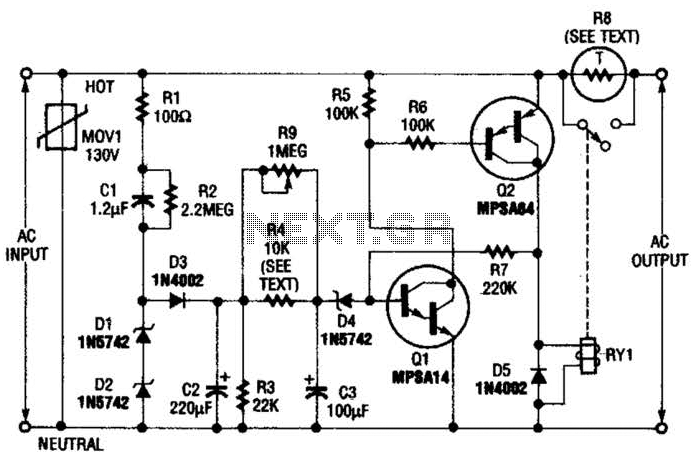
Q1 is an NPN Darlington transistor, and Q2 is a PNP Darlington transistor. MOV1 is a metal-oxide varistor, while R8 is a thermistor used for limiting inrush current. This circuit is designed to limit AC line current to a...

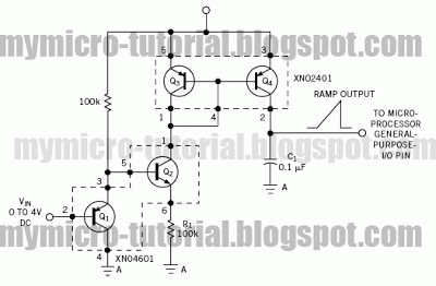
A voltage-controlled oscillator (VCO) operates similarly to a voltage-to-frequency converter (VFC). Its output frequency is determined by a control voltage input. In the circuit diagram, 'd' represents the amplifier input voltage, which is set to 0.6V, while 'h' denotes...
This circuit is a conventional Pierce type oscillator that utilizes a JFET. It employs fundamental mode crystals and demonstrates good performance and reliability when a low noise JFET is used. The feedback is regulated by the capacitance C1, which...
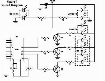
It consists of a 4047 low-power monostable/astable multivibrator, IC1, used in the astable mode to provide the timing pulses to control the flash rate of the LEDs. To accomplish the astable mode, pins 4, 5, 6, and 14 are...
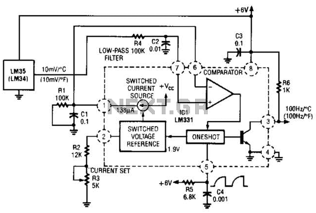
In this circuit, an LM34 or LM35 generates a frequency that is proportional to temperature. The reference current (138) is established through resistor R3. The output can be utilized to drive a display, frequency counter, or other indicating devices...
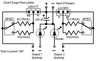
Here is a deluxe version of the simple charge rate limiter, using the same idea but with the ability to charge two packs simultaneously from a single wall charger. For circuit description and parts list, see the simple charger...