
0-40V lab power supply circuit diagram electronic project using LM723 L146

The adjustable laboratory power supply circuit is designed to provide a versatile and reliable source of DC voltage for various electronic applications. The LM723 voltage regulator is a well-established component known for its ability to maintain a stable output voltage, while the L146 offers enhanced performance for higher voltage applications. The circuit is configured to allow for fine-tuning of both voltage and current outputs, making it suitable for testing and powering a wide range of devices.
The circuit diagram highlights the integration of a resistive network that effectively mitigates the minimum output voltage limitation typically associated with integrated circuits. By employing potentiometer P2, users can achieve a full range of output voltages down to zero, which is particularly beneficial for applications requiring precise voltage control.
The choice of capacitors in the circuit is critical as they must be selected based on the required output characteristics, including ripple voltage and load stability. Additionally, the power dissipation must be carefully monitored to ensure that the transistors do not exceed their thermal limits. The inclusion of parallel 2N3055 transistors allows for greater current handling capabilities, which is essential when powering devices that require higher currents. This configuration, however, demands a transformer capable of supplying sufficient current, thereby ensuring the overall stability and reliability of the power supply.
In summary, this adjustable power supply circuit is a robust solution for laboratory environments, providing flexibility in voltage and current outputs while ensuring safe operation through careful component selection and configuration.A very lab adjustable power supply that can provide an output voltage between 0 and 60 volts can be designed using this circuit diagram. This lab power supply can be designed with LM723 chip or for higher output voltages, with L146. Output current is also adjustable, but once established, is always effective. Table 1 shows the values to be modif ied to have three different versions of the maximum output voltage (30, 40 and 60 V). Electrical diagram below shows the alternative 40 V / 0. 8 using L146 chip because it can stabilize higher output voltage, much better than the LM723. Normally, 2 V is the minimum voltage stabilized that even an integrated circuit can provide. Resistive network R3, R4 and R5, R6 "kill" this restriction so that output can be set to 0 V with potentiometer P2. Depending on the output requirements, will be decided on the type and the semiconductor capacitors to be used.
Output current must be limited so as to keep power dissipation of 40 W. T3 under maximum output current for 40 V version is 0. 8 A. It can connect two parallel 2N3055 transistors (with emitter resistors) to double the current output, but in this case requires a 2 A transformer 🔗 External reference
Related Circuits
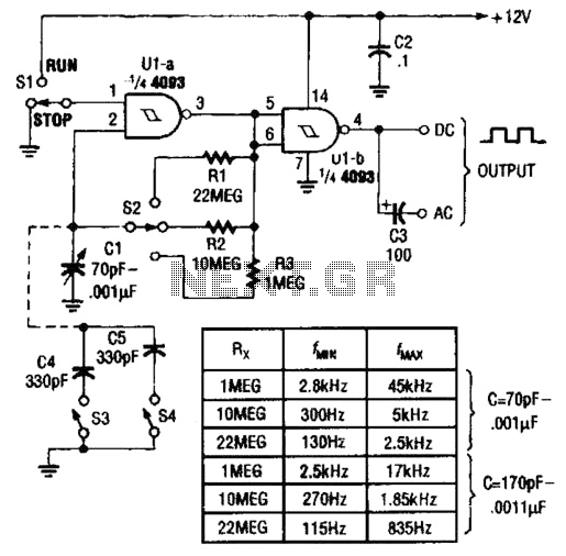
Two gates of a Quad 4093 are utilized in an astable multivibrator configuration. CI is a three-gang 365 pF variable capacitor with its sections connected in parallel. Additionally, S3 and S4 serve to switch in optional extra capacitors. The described...
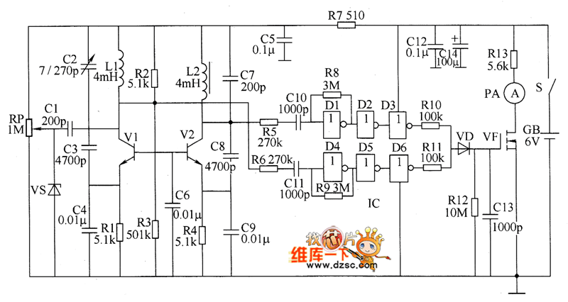
The metal detector circuit consists of several key components including the probe oscillator, reference oscillator, oscillation signal processor, mixing amplifier, and ammeter PA. The probe oscillator is made up of the oscillating tube VI, exploration coil L1, capacitors C1...
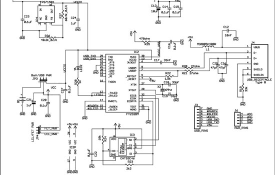
As found in SLAA458, the revised pulse oximeter application, an image of the USB schematic is attached, which is used to output collected data. There are a few questions regarding this schematic: 1) What do J3 and J6 correspond...
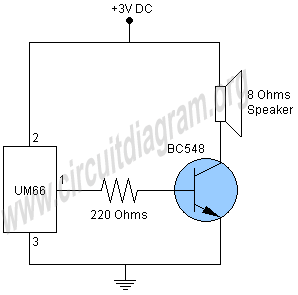
This project involves a simple doorbell circuit featuring the UM66 melody integrated circuit (IC), which is well-known for its melody generation capabilities. The IC is housed in a TO-92 transistor package and consists of only three pins, functioning as...

High-order filters are typically designed with two or more cascaded sections. An order 4 filter requires only one operational amplifier integrated circuit (OA IC), allowing for lower distortion. High-order filters are essential in various applications, including audio processing, signal conditioning,...

This FM IF MW radio receiver circuit schematic utilizes the LA1260 integrated circuit (IC), which is suitable for AM and FM radio receiver electronic projects. The LA1260 incorporates numerous functions and features essential for radio receiver applications, including a...