
Arduino Audio DAC Options

The digital-to-analog conversion process is critical in applications where digital signals need to be transformed into analog waveforms, such as audio signal generation. The DAC's ability to modulate output voltage levels based on digital input allows for precise control over sound characteristics. The PWM-based DAC implementation is particularly advantageous due to its simplicity and cost-effectiveness, making it suitable for hobbyist projects and educational purposes. The choice of an 8-bit resolution provides a balance between sound quality and processing complexity, while higher resolutions can be explored for applications requiring finer audio fidelity. The inclusion of sound samples serves to illustrate the practical differences between various DAC configurations, providing a valuable reference for users to understand the impact of bit resolution on audio output. Furthermore, the software abstraction layer enhances flexibility, enabling users to switch between different DAC types without significant code alterations. This modularity is essential for rapid prototyping and experimentation in sound synthesis projects. The circuit design, featuring AC coupling and filtering, is crucial for ensuring clean audio output, avoiding distortion, and maintaining signal integrity. Overall, the exploration of DAC options, particularly in a microcontroller environment like Arduino, showcases the versatility and potential of digital-to-analog conversion in modern electronics.DAC is short for Digital to Analog Converter. In this article we play around the code Michael Smith created for a PWM based DAC. I modified his code so that other DAC options could be tried. I compare the 8-Bit PWM DAC with the R2R DAC at various numbers of bits. You might be surprised at how well a 4-bit DAC sounds. This article includes several sound samples for the various DAC options and demonstrates some software abstraction that allows for multiple DAC options. This article is part of the series on Arduino Sound Generation. I decided to drop the Part 1, 2, 3 distinction as much of the content is not dependent on the previous articles.
Of all the various methods of sound generation the DAC method seems most versatile to me. As mentioned before DAC is a common short name for Digital to Analog Converter. Basically a binary/digital value is converted to an analog/voltage value. An 8-Bit DAC would convert a binary value in the range of 0 to 255 into an analog voltage from 0 to 5V. The exact voltage range of the conversion is dependent on the DAC configuration but for most things we will play with, 0 to 5V will work.
Since analog signals, especially sound, needs to swing plus and minus around 0V we often bias the DAC so that mid scale is considered 0V. If the DAC outputs from 0 to 5V then we usually bias the signals so that 2. 5V is translated to 0V. If we generate our output signals so that half scale is 2. 5V then we can AC couple the output to get a +/- 2. 5V swing. The half scale biasing may be a bit confusing but really it`s easy once you get the general idea. We just call 1/2 scale zero so that any numbers above 1/2 are positive and below are negative. For an 8 bit converter we can use the MSB as a sign bit to make this happen. Consider that decimal 128 is 10000000 in binary. Note that the MSB is set and this is basically half scale of the possible 0-255 range. Think of the MSB as a sign bit, it`s one for positive values and 0 or negative. Using this 1/2 scale bias we can convert any digital number that might represent sound data into a value to load into a DAC.
The first step is to convert the number into the range of +/-127 and add 128 to it. In this example that will make the analog version swing from 0 to 5V with the original zero point set at 2. 5V. We can remove that 2. 5V bias in the hardware with a simple series capacitor. The series capacitor is not even needed in most applications. For example I use my sound card line input to do these experiments. This input has a series capacitor. The series capacitor is used to provide A/C coupling. This just means that the signal swings evenly around 0V. The +/- voltage swing is enforced about the average DC level by the capacitor. Of course there is a frequency response for the series capacitor but the value of the capacitor is usually high enough so that it will not be a problem for audio frequency ranges.
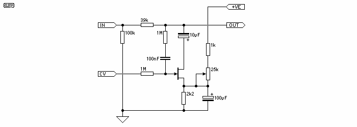
This diagram shows the circuit I used between the various DAC outputs and my PC sound card input. The series resistor and capacitor to ground form a simple filter to knock off the high frequency noise caused by the DAC switching instantly between the voltage values. It removes the high frequency components. The 100K variable resistor (POT) lets me adjust the output voltage level for each DAC. A line input should be kept in the 1V Peak to Peak range or +0. 5 to -0. 5 range. Since the sound card has A/C coupling I only need to adjust the amplitude using this POT as a voltage divider.
Also note that I connected both the right and left side inputs to the filtered output. 🔗 External reference
Related Circuits
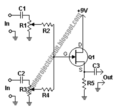
The circuit devised by Phil Allison still has some input voltage limitations, since it is based on a FET. Junction FET VCAs also create considerable distortion, with the worst of it appearing when the signal is attenuated by 6dB....
This project involves a simple circuit designed to mix two or more audio channels into a single channel, such as converting stereo audio into mono. The circuit is capable of accommodating multiple input channels while maintaining low power consumption....
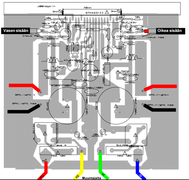
This amplifier is of such high quality that it would be an understatement to call it a HIFI amplifier. According to HIFI-confirmed-Finland, the frequency response must be direct and distortion <1% 20-20 kHz. Our power amplifier circuit meets the above requirements for bandwidth 5Hz - 500 kHz, however, the frequency band is limited to prevent interference. The amplifier meets the requirements for a reference amplifier, which is suitable for measurement and comparison operations. Small 12-24V voltage system amplifiers operating in the power and properties are somewhat modest, for instance, testing decent speakers. The amplifier is also suitable for demanding PA use. When music occurs at shallow close 20Hz sound levels, the whole amplifier power reserve may need to be temporarily used. This happens especially when the low-frequency emphasis equalizer or amplifier is used, for example, TV. Watching a movie with lots of sound effects, if the power is not enough in that situation, the sound from the speakers is distorted, reducing the enjoyment of hearing or even damaging the speaker drivers. The distortion of human hearing range is only about 20 Hz-20 kHz. The hi-fi speaker gamut extends at its best to 25kHz and the hearing area of bats "remains" at 150 kHz, so what are the practical benefits of the amplifier's superior frequency characteristics? The power of less than 1% distortion mentioned in the title 220W blue means the so-called total maximum amount of distortion. This includes TIM distortion (Transient intermodulation) as well as IM-distortion (intermodulation-distortion). TIM distortion occurs in connection with high-speed percussion sounds, such as the sound of dishes on drums. If the amplifier's share of this distortion is high, the amplifier will not be able to play the sound clean, but the sound will be distorted. The higher the frequencies the amplifier is capable of playing, the less is TIM distortion. If the amplifier would be able to repeat 600 kHz, distortion would not occur at all. IM distortion means that the amplifier generates excess denominated, the so-called undesirable ghost signals. For example, fed in to 19 kHz. And 20 kHz, consists of the difference between 1kHz. Safety Because this amplifier has AC parts, its construction is permitted only in the technical work of teachers. Even in this case, the device should be checked by experts before connecting it to the network. Although the equipment has been revised, it is worth remembering that even the only speaker outputs may at best affect almost 70V the effective voltage. Therefore, caution is necessary during building and operation. For instance, the speaker terminals should be protected against contact. Building instructions and testing of the amplifier circuit board components will be worth and an amplifier solder test in three stages: 1) The components of the power side, and all the cables signal cables except installed 2) any other circuit board components plus not only hybrid circuit STK 4231 3) STK 4231 placed and cooled, and the input signals the wires connected. Installation of the power-side components and testing should be done carefully. The transformer wires insulation must first be removed carefully or checked that this has already been done. Then the transformer conductors order is checked on the transformer side. The circuit board parts include STK4231II Hybrid, Led green, resistors of different values, ceramic and plastic capacitors, a rectifier, fuse holders and fuses, a coil, line voltage parts, potentiometer, RCA connectors, speaker output screws, and a cooling unit.
These accessories are low-cost, high-speed, bifet-input operational amplifiers utilizing internally compensated voltage (BI-FET II technology). They require low supply voltages while offering a wide gain bandwidth product and fast slew rate. Additionally, well-matched high voltage JFET input devices accommodate...
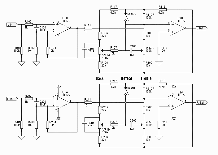
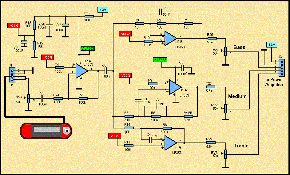
The sound system features a de-sensitized design with a maximum range that can be increased if desired. It includes two tone controls: one offering a lift of 10 dB and the other providing a subtle cut of 3 dB....
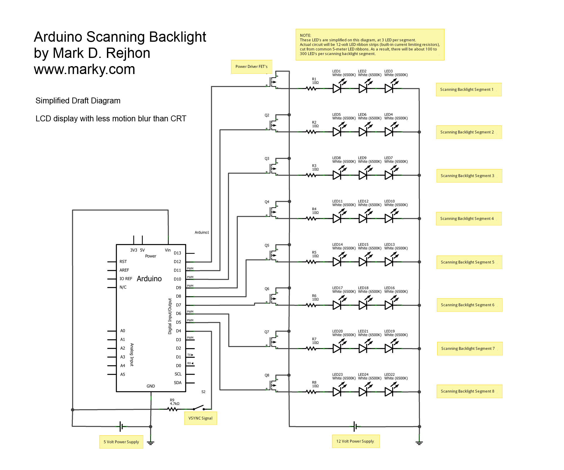
This is a simplified schematic diagram for a homemade scanning backlight driven by an Arduino, an open-source electronics prototyping platform. The Arduino monitors the VSYNC signal (input-lag compensated) and executes a backlight scanning sequence, using ultra-short strobes of super...