
The NOT gate
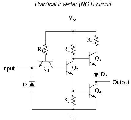
To analyze this circuit under the condition where the input is "high," or in a binary "1" state, the input terminal can be connected to Vcc through a switch. In this scenario, diode D1 will be reverse-biased and will not conduct any current. The inclusion of D1 in the circuit serves to protect the transistors from damage in the event of a negative voltage being applied to the input (a voltage that is negative relative to ground). With no voltage applied between the base and emitter of transistor Q1, it would be expected that no current would flow through it. However, Q1 operates differently in this circuit, functioning as a back-to-back pair of diodes.
The purpose of these diodes is to direct current to or away from the base of transistor Q2, depending on the input logic level. Understanding how these two diodes "steer" current may require an illustrative example. Consider a diode/resistor circuit that represents the base-emitter junctions of transistors Q2 and Q4 as single diodes, allowing for a focused analysis of the current "steered" through the back-to-back diodes. When the input switch is in the "up" position (connected to Vcc), it is evident that there will be no current through the left steering diode of Q1, as there is no voltage across the switch-diode-R1-switch loop to drive electron flow. However, current will flow through the right steering diode of Q1, as well as through the base-emitter junctions of Q2 and Q4. This indicates that in the actual gate circuit, transistors Q2 and Q4 will receive base current, allowing them to conduct collector current.
The total voltage drop between the base of Q1 (the node connecting the two back-to-back steering diodes) and ground will be approximately 2.1 volts, which corresponds to the combined voltage drops of three PN junctions: the right steering diode, Q2's base-emitter diode, and Q4's base-emitter diode. If current were measured in this circuit, it would be observed that all current flows through the left steering diode of Q1, with none passing through the right diode. This raises the question of why there appears to be a complete path for current through the diodes of Q4 and Q2, the right diode of the pair, and resistor R1, yet no current flows through that path.
The explanation lies in the nonlinear characteristics of PN junction diodes; they do not conduct current until a certain forward voltage is applied, which is approximately 0.7 volts for silicon diodes and 0.3 volts for germanium diodes. Once they begin conducting, they maintain a voltage drop of about 0.7 volts. When the switch is in the "down" position, the left diode of the steering diode pair conducts fully, dropping approximately 0.7 volts across it. In contrast, with the switch in the "up" position (where transistors Q2 and Q4 are conducting), a total of about 2.1 volts is dropped across the relevant components, illustrating the circuit's operation and the role of each component in the logic gate function.The single-transistor inverter circuit illustrated earlier is actually too crude to be of practical use as a gate. Real inverter circuits contain more than one transistor to maximize voltage gain (so as to ensure that the final output transistor is either in full cutoff or full saturation), and other components designed to reduce the chance of acc
idental damage. This circuit is composed exclusively of resistors and bipolar transistors. Bear in mind that other circuit designs are capable of performing the NOT gate function, including designs substituting field-effect transistors for bipolar (discussed later in this chapter). Let`s analyze this circuit for the condition where the input is "high, " or in a binary "1" state. We can simulate this by showing the input terminal connected to Vcc through a switch: In this case, diode D1 will be reverse-biased, and therefore not conduct any current.
In fact, the only purpose for having D1 in the circuit is to prevent transistor damage in the case of a negative voltage being impressed on the input (a voltage that is negative, rather than positive, with respect to ground). With no voltage between the base and emitter of transistor Q1, we would expect no current through it, either.
However, as strange as it may seem, transistor Q1 is not being used as is customary for a transistor. In reality, Q1 is being used in this circuit as nothing more than a back-to-back pair of diodes. The following schematic shows the real function of Q1: The purpose of these diodes is to "steer" current to or away from the base of transistor Q2, depending on the logic level of the input.
Exactly how these two diodes are able to "steer" current isn`t exactly obvious at first inspection, so a short example may be necessary for understanding. Suppose we had the following diode/resistor circuit, representing the base-emitter junctions of transistors Q2 and Q4 as single diodes, stripping away all other portions of the circuit so that we can concentrate on the current "steered" through the two back-to-back diodes: With the input switch in the "up" position (connected to Vcc), it should be obvious that there will be no current through the left steering diode of Q1, because there isn`t any voltage in the switch-diode-R1-switch loop to motivate electrons to flow.
However, there will be current through the right steering diode of Q1, as well as through Q2`s base-emitter diode junction and Q4`s base-emitter diode junction: This tells us that in the real gate circuit, transistors Q2 and Q4 will have base current, which will turn them on to conduct collector current. The total voltage dropped between the base of Q1 (the node joining the two back-to-back steering diodes) and ground will be about 2.
1 volts, equal to the combined voltage drops of three PN junctions: the right steering diode, Q2`s base-emitter diode, and Q4`s base-emitter diode. If we were to measure current in this circuit, we would find that all of the current goes through the left steering diode of Q1 and none of it through the right diode.
Why is this It still appears as though there is a complete path for current through Q4`s diode, Q2`s diode, the right diode of the pair, and R1, so why will there be no current through that path Remember that PN junction diodes are very nonlinear devices: they do not even begin to conduct current until the forward voltage applied across them reaches a certain minimum quantity, approximately 0. 7 volts for silicon and 0. 3 volts for germanium. And then when they begin to conduct current, they will not drop substantially more than 0. 7 volts. When the switch in this circuit is in the "down" position, the left diode of the steering diode pair is fully conducting, and so it drops about 0.
7 volts across it and no more. Recall that with the switch in the "up" position (transistors Q2 and Q4 conducting), there was about 2. 1 volts dropped between those same two poin 🔗 External reference
Related Circuits
A comprehensive design procedure is proposed for the development of Field-programmable/Reconfigurable Analog Integrated CMOS circuits. Instead of relying on iterative simulation steps to meet design specifications by adjusting the W/L ratios of the FETs, first-order classroom equations are utilized...
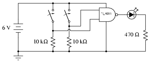
To start, connect a single NAND gate to two input switches and one LED, as illustrated. Initially, using an 8-position switch and a 10-segment LED bar graph may appear excessive, given that only two switches and one LED are...
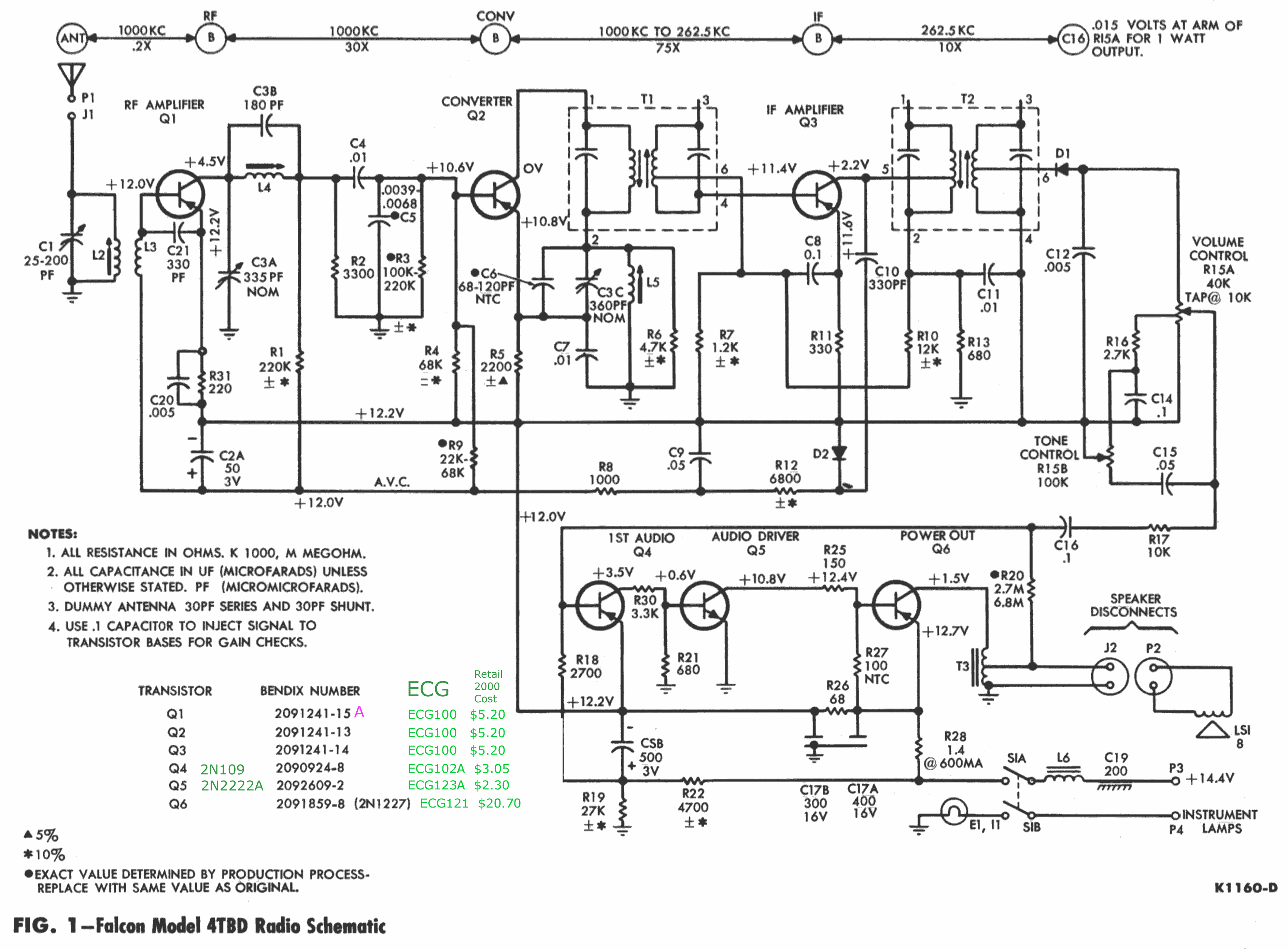
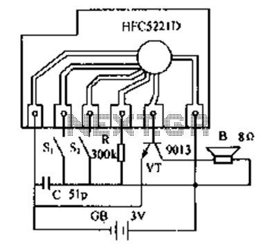
The chassis externally resembles the 22BD model, with the exception that the 22BD features a jack for speaker connections—two female sockets—located on the right (antenna) side. In contrast, the 3BTD model has a 3-inch harness (black and green wires)...
Do not drink and drive. Wishing you a safe journey home. Language Integrated Circuits. Language Integrated Circuits (LICs) are specialized electronic components designed to facilitate the processing of language-based data within various applications. These circuits integrate multiple functions, such as...
The ASUS Eee is an exceptional ultra-portable notebook that includes nearly all the necessary features for technology enthusiasts while omitting unnecessary elements. Additionally, it boasts an impressive build quality. The ASUS Eee series is designed with portability and functionality in...
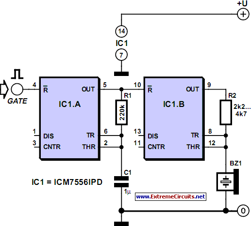
Occasionally, a simple gated pulsed alarm is required. The circuit presented here utilizes only four components along with a piezo sounder, making it highly efficient in terms of simplicity. While it may not produce the most powerful output, it...