
Field-programmable Operational Transresistance Amplifier using Floating-gate MOSFETs
The growing demand for mobile communications has necessitated high levels of chip integration and directed research towards high-frequency applications. Traditional voltage operational amplifiers are inadequate for new circuit topologies designed for high-frequency signal processing due to their closed-loop gain-dependent bandwidth, making current-mode approaches more favorable. Current-mode circuits offer advantages over voltage-mode counterparts, including wider bandwidth, higher slew rates, greater linearity, and lower power consumption, thus making them suitable for high-frequency operations.
The operational transresistance amplifier (OTRA) is a three-terminal analog building block with properties similar to current-feedback operational amplifiers (CFOA) but with two low-impedance inputs and one low-impedance output. OTRAs, often referred to as Norton amplifiers, have garnered attention for their advantages in current-mode circuit design. However, existing commercial implementations do not provide a true virtual ground at the input terminals, limiting functionality and requiring complex designs with external DC bias currents.
To address these limitations, various topologies have been proposed, although they tend to be complex and do not function effectively at low power supplies. The design of a high-performance CMOS differential OTRA is essential for current-mode analog system design, characterized by low impedance at both input and output terminals. This feature makes circuits insensitive to stray capacitances, ideally allowing the transresistance gain to approach infinity and equalizing input currents through external negative feedback.
The proposed design procedure leverages FGMOS technology to introduce non-volatile, high-precision on-chip programming capabilities in the OTRA design. This approach allows for post-fabrication tuning of critical specifications to meet desired values within a specific range using analog voltages, eliminating the need for additional circuitry for tuning. FGMOS devices permit continuous variation in threshold voltage by storing charge in a non-volatile memory, maintaining the stored charge for over a decade.
The design emphasizes low power consumption and thermal stability, with the total power dissipation and output voltage variation with temperature being critical considerations. This methodology can be applied to various analog integrated circuits, demonstrating the potential for programmability in analog designs. The advancements in floating gate technology have shifted the paradigm in analog circuit design, enabling real-time, non-volatile, and reconfigurable programming capabilities, which are vital for modern electronic applications.We propose a comprehensive design procedure to design Field-programmable/Reconfigurable Analog Integrated CMOS circuits. Instead of repeatedly iterative simulation steps to achieve desired design specifications by fine tuning the W/L ratios of the FETs, we use first order classroom equations to achieve central value of desired specifications and t
hen execute a customized fine tuning of specifications to the customers requirement with the help of Floating-gate Transistors FGMOS. To demonstrate the proposed design cycle, a modified high frequency/RF Operational Transresistance Amplifier (OTRA) CMOS circuit is designed where transresistance gain and input output low impedances are programmable, independently to desired values within a specific field range, using FGMOSs.
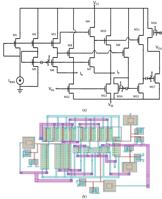
In FGMOS the programmable charge at floating-gate using external voltages can results in threshold voltage field-programming, which in turn program the design (OTRA) specifications. With specific sizing and biasing condition, the transresistance can be programmed from 0. 5kohm to 6kohm, input and output impedance from 600ohm to 10Kohm, while offset current can also be compensated independently using respective FGMOSs with 13-bit programming precision.
However the final circuit, with four FGMOS occupies 75 µm G— 64 µm chip area. The design also consumes less power, total power consumption is about 3. 96mW and show good thermal stability as output voltage variation with temperature is about 25 µV/ °C. Cite this paper: Garima Kapur, Sajal Mittal, CMMarkan, VPPyara, Design of Field-programmable Operational Transresistance Amplifier using Floating-gate MOSFETs, Microelectronics and Solid State Electronics, Vol.
2 No. 2, 2013, pp. 11-23. doi: 10. 5923/j. msse. 20130202. 01. The growing demand for mobile communications has led to high level of chip integration and directed research towards the field of high frequency applications. In the new designed circuit topologies for high frequency signal processing conventional methods based on voltage op-amp are no longer adequate as op-amp has a closed-loop gain dependent bandwidth, thus current-mode approach is preferred.
Current mode circuits has potential advantages over their voltage counterparts, such as their inherently wide bandwidth, higher slew-rate, greater linearity, wider dynamic range, simple circuitry and low power consumption[1] and hence suitable for high frequency operations. In 1985 the popularity of current feedback op-amp amplifiers (CFOA) has increased considerably as they were found to be able to overcome the limitations arising from conventional operational amplifiers[2].
The term current-feedback is used because the error signal entering at the feedback node of the op-amp is in the form of a current and this gives to the amplifier a constant closed loop bandwidth capability[3]. Since the CFOA has a larger bandwidth and a higher slew-rate than the conventional op-amp, analog signal processing circuits built around the CFOA are expected to operate at higher frequencies than the op-amp based circuits[4].
An alternate current-mode circuit, operational transresistance amplifier (OTRA), is a three terminal analog building block shown symbolically in Figure 1(b) and defined using matrix, shown in Figure 1(b)[5]. It has similar transmission properties to the current-feedback op-amp, with an addition of two low-impedance inputs and one low-impedance output.
OTRA, which is commercially available under the name of Norton amplifier (like Z10040A Norton noiseless feedback Amplifier[6]) have been attracted attention by its advantages in the current-mode circuit design. These commercial realizations do not provide a true virtual ground at the input terminals and they allow the input current to flow in one direction only.
The former disadvantage limited the functionality of the OTRA whereas the latter forced to use external dc bias current leading complex and unattractive designs[7]. In order to remove these disadvantages of the OTRA, some topologies are proposed in the literature[8-10].
But these solutions are both complex structures and they do not operate properly at low power supplies, however in future design concept the main interest is designing circuitries with low power supplies. This demand leads designing a high performance CMOS differential OTRA for the current-mode analog systems design[11-14].
In CMOS OTRA design both the input and output terminals are characterized by low impedance. The input terminals are virtually grounded leading to circuits that are insensitive to stray capacitances[5]. Ideally the transresistance gain, Mr. , approaches infinity, and applying external negative feedback will force the two input currents I+ and I ’, to be equal (see Figure 1).
This leads to growing interest for the design of OTRA-based analog signal processing circuits, such as instrumentation amplifiers MOSFET-C differentiator, integrators, continuous-time filters, immitance simulators, waveform generators, bistable multivibrators, oscillators[15-24]. A low-pass, band-pass, high-pass, and band-reject biquad filter is proposed using two OTRAs, three capacitors, and several resistors[19].
The phase shifter uses n-OTRA is tunable and blocks to give a total of n+1 oscillation[20]. A voltage-mode proportional-derivative using single OTRA, two resistors and a capacitor, having orthogonally tunable proportional and derivative constants[25] is proposed. Similarly a single OTRA with a capacitor and five resistors are used to propose a grounded negative inductance emulator with full independent control on both the inductance value and the condition[10].
These circuits require additional circuitry to introduce tuning ability within them. Thus programmable devices are required for accurate prototyping/on-chip tuning ability of the design. These circuits also experience limitation in applications like in highly integrated portable electronic devices, where less power consumption and small size hardware with higher integration is required.
Moreover, there are various electronic systems where high precision tuning ability/programmability is required like for biologically inspired circuits such as bionic ear processor, learning circuits and related adaptive filters, neuromorphic and cellular computing circuits, etc. Instead of using additional circuitry we would like to modify the basic OTRA CMOS circuit[5] using Floating-gate Transistors (FGMOS) in place of conventional MOS, to introduce non-volatile, high precision on-chip programming in the OTRA design.
The circuit is designed using a comprehensive design procedure which allows post fabrication and independent tuning of critical specifications to desired values within a specific field range using analog voltages. Thus we propose a design procedure where instead of repeatedly iterative simulation steps to achieve very precise design specifications by fine tuning the W/L ratios of the FETs, we use first order classroom equations to achieve central value of desired specifications and then execute a customized fine tuning of specifications to the customers requirement.
While maintaining small size and low power consumption, FGMOS are introduced in place of conventional MOS device hence conductivity of a MOS can be corrected by altering its threshold voltage (VT) by a field user[26, 27]. The OTRA circuit is analysed and derived in terms of design specifications whose derived equations show direct dependence on MOS thresholds.
FGMOS offers continuous variation in threshold by storing the weights in a non-volatile analog memory with high accuracy[28, 29, and 30]. And the charge once stored at FG can be retained for more than 10 years. The proposed programmable OTRA design will not required extra hardware for storing, no digital code controlling circuitry however it will require interconnects to provide desired analog voltages to program floating gates of respective FGMOSs.
In paper, parametric analysis of each OTRA design specification with respect to respective MOS is performed and hence, the circuit is modified with FGMOSs, which provide independent programming ability of design specification as well as circuit offsets, after fabrication. The total power dissipation and thermal stability of the modified design is also being catered in the paper.
Such consistent approach to introduce programmability can be applied to various analog ICs (the idea of programmability using floating gate transistor is being published in conferences before[31, 32 and 33]). Although vigorous development of consumer electronic products has been propelled by advancements in digital processing technology, the world is still analog.
Sound, video and image are always represented in the form of analog signals. Analog designs tend to have higher integration density, consume less power and interface easily with the real world yet they are still less preferred option compared to their digital counterparts as analog implementation lacks accurate convertibility of design to prototype, stability of devices, long term storage of analog signals, field programmability and automated design. Analog design is more concerned with the physics of the semiconductor devices such as gain, matching, power dissipation, and resistance.
However, fidelity of analog signal amplification and filtering is usually critical and as a result, analog IC design is critical. Thus there is a drive towards shorter design cycles for analog integrated circuits, which demand the development of high performance analog circuits that are reconfigurable and suitable for CAD methodologies[34].
Several manufactures have made programmable analog circuits; among these are Motorola, IPM Inc, Lattice and Anadigm. Several designs of Field Programmable Analog Arrays (FPAA) have been reported[35]-[38], but these are often aimed at a commercial market as an analog counterpart to Field Programmable Gate Arrays (FPGA) for rapid prototyping of analog circuits.
Subsequently to introduce programmability in analog designs programmable device are also developed such as various methods are developed to modify electrical characteristics of MOS device which in turn introduce programming ability in MOS. It is performed either through openings in the passivation layer to define location of bonding pad or through ion implantation at exposed underlying polysilicon gate structure which create an implantation layer at the channel regions of selected MOS devices, and thereby permanently alter the threshold voltages of these MOS devices[39, 40].
However over the last decade there is a new technology based on floating gates have developed and floating gate circuit approaches have progressed from a few foundational academic results to stable circuits. Floating gate MOS are like conventional MOS with an additional gate in which by modifying the charge at the floating gate MOS characteristics (threshold) can be programmed on-chip after fabrication with real time, non-volatile, reconfigurable programming[41-43].
This programmable analog technology empowers analog signal processing approaches programmable precision analog low-power techniques[44]. Moreover as we move into more advanced CMOS process nodes, it has become apparent to the designers that although the fundamental RF/analog design principles remain unchanged, there have to be new techniques and architectures to fully harness the potential of CMOS scaling and to advance the state of the art.
So inspired from floating gate MOS technology, we would like to propose a paradigm shift in analog circuit designing where instead of repeatedly iterative simulation steps to achieve very precise design specifications by fine tuning the W/L ratios of the FETs, we use first order classroom equations to achieve central value of desired specifications and then execute a customized fine tuning of specifications to the customers requirement. The proposed analog design cycle flowchart and algorithm is illustrated in Figure 2. As conventional Analog design cycle consists of basic five steps: system modelling, circuit simulation, layout, physical verification and post layout verification i.
e. it is useful to first model the behaviour of those system to understand its stability conditionand system response, then for targeted specifications some changes such as architectural change in circuit, resizing of transistors might be needed. This can be achieved by manual design, table-based calculation employing Excel or Matlab, circuit sizing by Genetic Algorithms or Particle-Swarm- Optimization or by circuit simulations like SPICE.
However, troubleshooting of each stepisvery complicated. It is aloop linked back to the previous steps and possibly troubleshooting all the way back to step1. 🔗 External reference
Related Circuits
A small signal amplifier, perhaps of the type to follow the previous buffer amplifier. We will assume we are buffering and amplifying our signal from the voltage controlled oscillator tutorial. In those examples we were generating and buffering 1.8...

The following diagram is the circuit diagram of a 20W power amplifier built using the tube component EL34. The EL34 is a well-known tube, ideal for power tube amplifiers. The circuit presented is a complete design that includes both...
Using just two NAND or inverter gates, it is possible to build a D-type (or toggle) flip-flop with a push-button input. At power-up, the output of gate N2 is at a logical 1, ensuring that transistor T2 is switched...
The circuit works from a symmetrical -40 VDC power supply and draws a maximum current of 2.6 A. The input circuit of the amplifier is a differential amplifier built around Q4 and Q5 that employ DC feedback thus preventing...

A common emitter amplifier is a total pole amplification circuit structure featuring a key emitting device. This circuit refers to the emitter of the input signal and the output signal connected to a common ground, forming the basis of...

This differential amplifier utilizes a CA3193 BiMOS operational amplifier. It serves as a classical differential input-to-signal-ended output converter, which, when paired with a low-resistance signal source, will sustain a high common-mode rejection ratio (CMRR), provided that R1 equals R3...
Warning: include(partials/cookie-banner.php): Failed to open stream: Permission denied in /var/www/html/nextgr/view-circuit.php on line 713
Warning: include(): Failed opening 'partials/cookie-banner.php' for inclusion (include_path='.:/usr/share/php') in /var/www/html/nextgr/view-circuit.php on line 713