High-quality DAC converter from USB to S/PDIF. The circuit utilizes the PCM2704 chip, which was provided as a sample by Texas Instruments. It features an analog output for headphones and a digital S/PDIF output with both electrical and optical (TOSLINK) interfaces. Additionally, it incorporates three Human Interface Device (HID) buttons for volume control and muting. The schematic closely follows the PCM2704 datasheet. The circuit includes components such as the DAC, S/PDIF output, and HID buttons. For USB input, a standard mini USB connector is used, while the headphone output employs a standard 3.5mm stereo jack socket. A RS-485 bus transceiver is utilized to convert signals from TTL level to a differential signal, and an optical transmitter, TOTX173 from Toshiba, is used for the optical output. The assembly process begins with drilling holes for the crystal, wires, connectors, and buttons. The integrated circuit PCM2704 is then positioned, soldering one pin in the corner before proceeding to solder all pins on the opposite side with thin solder. The first side is also soldered, and if any pins are shorted, copper solder wick is used to remove excess solder. The presence of sufficient colophony allows for automatic unjoining of pins due to surface tension. The circuit board is populated with the 75176B chip, SMD resistors, and capacitors, which are soldered in place by holding them with a nail, small screwdriver, or tweezers. After ensuring proper positioning, components are soldered on both sides of the board. The SMD connector and wire junctions are soldered last. The circuit operates immediately upon connection to a computer, recognized as a standard USB sound card. No drivers are required for common operating systems like Linux or Windows XP. The volume settings can be adjusted using the buttons. The PCB is designed for single-sided use with two wire junctions in the Eagle 5 application, with most components and the USB connector mounted on the bottom side and wire junctions, buttons, inductor, crystal, and remaining connectors on the top side. The design aims to separate the analog and digital sections to minimize interference. The S/PDIF (Sony/Philips Digital Interface) is intended for the transmission of digital audio signals, with a professional variant known as AES3. Both protocols share similar characteristics with some exceptions, such as copy protection in commercial S/PDIF. The commercial variants include electrical with TTL output (for example, CD-ROM), electrical with a voltage level of 0.5Vpp on a cinch (RCA) connector using coaxial cable with 75Ω impedance, typically found in consumer devices, and optical TOSLINK from Toshiba. All three transmission methods utilize identical signal encoding, allowing conversion between them. The transfer speed depends on sample frequency, bit depth, and the number of channels. In addition to basic uncompressed PCM encoding, the interface is also utilized for transmitting encoded multichannel audio formats such as Dolby Digital and DTS. The advantage of this interface is that only one wire is needed for complete audio signal transmission; however, this can also be a disadvantage, as the receiver must reconstruct the clock signal from the data using a Phase-Locked Loop (PLL), which can introduce jitter, perceived as distortion in the output of the DAC. For digital audio transfer within equipment, the I2S bus is preferred. The circuit was built in two copies, both of which functioned correctly upon first connection. The analog output delivers good sound quality without interference, surpassing that of typical internal sound cards on PC motherboards. Low and mid frequencies are well represented, though high frequencies may appear slightly blurred. While it may not achieve Hi-Fi standards, the sound quality is generally sufficient for most users.High quality DAC convertor from USB to S/PDIF. I choose PCM2704 circuit, which sent me TI company like sample. Circuit has analog output for headphones and digital S/PDIF output with electrical and optical(TOSLINK) interface. We can use too 3 HID buttons for setting volume and mute. Schematics is almost identical to PCM2704 datasheet. Circuit includes these components: DAC, S/PDIF output and HID part with three buttons MUTE, VOL+ and VOL-. For USB input is used standard miniUSB connector. Headphone output uses standard 3. 5" stereo jack socket. For signal conversion from TTL level to differential signal is used RS-485 bus transceiver. For optical output is used optical transmitter TOTX173 from Toshiba. First I drill holes for crystal, wires, connectors and buttons. Next I settle intergrated circuit PCM2704, because I need more space for soldering. I put circuit on right place, solder one pin in the corner and next solder all pins on second side with thin tin. Next I solder first side. Effect is, that almost all pins are shorted. Next I must use copper solder wick for draining of tin out. If there are anough colophony that pins automatically unjoin thanks to surface tension. Next I put on the board circuit 75176B, SMD resistors and capacitors. These components I solder that after right position I hold them with nail, small screwdriver or tweezer.
One pin I solder with small amount of tin. If the component is on the right place, I solder them on the opposite side and finally on the first side. Next I solder SMD connector, wire junctions and finally all components from a top side. Circuit should work immediately after connection to computer. It is seen as standard USB soundcard. For usual operating systems like Linux or Windows XP are not needed any drivers. It should work too volume settings using buttons. PCB is designed for using only one side with two wire junctions in Eagle 5 application. Almost all components and USB connector are placed from bottom side. From top side are wire junctions, buttons, inductor, crystal and remaining connectors. I tried to separate analog part from digital and right place ground wires to eliminate interferences.
PCB is designed for easy creating in amateur conditions. S/PDIF [Sony/Philips Digital Interface] is designed for transfer of digital audio signal. There exists too professional variant AES3. Both use same protocol with few exceptions. Commercial S/PDIF has for example copy protection. There are also different voltage levels, connectors, impedance and transmission line (balanced/unbalanced). Commercial S/PDIF exists in three variants: Electrical with TTL output (for example CDROM), electrical with voltage level 0.
5Vpp on cinch (RCA) connector which use coaxial cable with impedance 75R commonly used on consumer devices and last optical TOSLINK from TOSHIBA. All three transfer methods have identical signal encoding and we can soever convert between them. Transfer speed is taken from sample frequency, number of bits and number of channels. Apart from basic uncompressed PCM encoding is interface today used for transferring of encoded multichannel audio for example Dolby Digital, DTS etc.
Advantage of interface is that only one wire is needed for transferring of complete audio signal. It is simultaneously disadvatage, because receiver must reconstruct clock signal from data with PLL and there can rise jitter, which is heared like a small distortion on the output of DAC. For transferring of digital audio within equipment is much better I2S bus. I built circuit in two copies and both works on first connection. Analog output has a good sound without interferences and he is better than usual internal soundcards on PC motherboards.
Low and middle frequencies are perfect, but highes frequencies are a little blurred. Just it isn`t HiFi, but for most people will be quality of sound output sufficient. I built this circuit pr 🔗 External reference
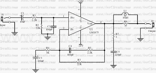
This simple 20 watts audio power amplifier is designed for home-brewed purpose. The L1 should be able to handle a current up to 4A to drive speaker in full load. The distortion is 0.015% @ 1KHz / 20W. This...
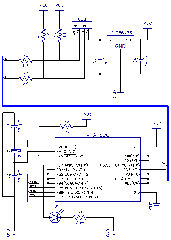
This is the second part of a USB tutorial for the ATtiny2313 microcontroller and the V-USB library. The first part covered how to derive 3.3V from USB to power circuits. In this section, the setup will be expanded with...
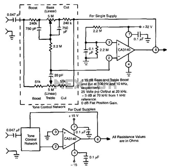
This circuit utilizes the high slew rate, high input impedance, and high output-voltage capability of the CA3140 BiMOS operational amplifier. It also offers mid-band unity gain using standard linear potentiometers.
The circuit design leverages the characteristics of the CA3140 BiMOS...
This design circuit functions to filter out interference signals, ensuring that the signal received from a Morse code station is distinct. The circuit utilizes the earliest mode of radio communications, which employs Morse Code on a continuous wave carrier...
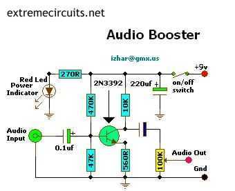
This small amplifier circuit is ideal for boosting small audio units.
The small amplifier circuit is designed to enhance the audio signals from low-output devices, such as microphones or portable music players. It typically employs a transistor or an operational...
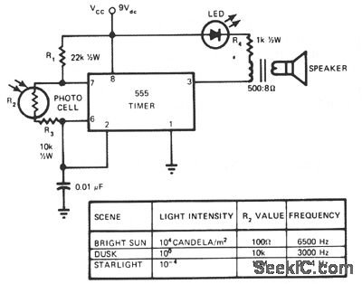
This circuit's frequency of oscillation increases directly with light intensity. The greater the light intensity, the higher the frequency of the oscillator. The 555 timer operates in astable oscillator mode, where frequency and duty cycle are controlled by two...
We use cookies to enhance your experience, analyze traffic, and serve personalized ads.
By clicking "Accept", you agree to our use of cookies.
Learn more