
Class AB output circuit diode coupling

The Class AB output stage circuit is designed to provide efficient amplification with reduced distortion. The configuration employs two transistors, VT1 and VT2, which work in tandem to manage the output signal across both positive and negative cycles. The biasing of VT1 is crucial as it sets the operating point, ensuring that the transistors are on the verge of conduction during idle conditions, thus minimizing crossover distortion.
The operation begins with the input signal U, which alternates between positive and negative cycles. During the positive half-cycle, the increase in collector current for VT1 reduces the voltage at points B and C, allowing for the emitter voltage to drop. The forward biasing of VD2 enables it to conduct fully, creating a path for the current to flow through the load resistor RL. This flow generates the output signal in the negative half-cycle.
Conversely, during the negative half-cycle, the collector current of VT1 decreases, which increases the voltages at points B and C. This condition turns on VT2, allowing it to conduct and connect VD2 to the positive supply voltage. This action creates a path for the output signal during the positive half-cycle, effectively mirroring the input signal's variations.
The use of diodes VD1 and VD2 plays a significant role in controlling the conduction states of the transistors. These diodes ensure that the transistors operate efficiently within their linear region, contributing to the overall performance of the amplifier. The careful design of the circuit, including the selection of resistor values and the configuration of the biasing network, is essential for achieving optimal performance and minimizing distortion in the output signal. Class AB output stage circuit coupled diode shown in Figure 10-8. Static, adjust VT1 bias circuit (not shown), so that the output at point E on the ground DC voltage UE o. The forward voltage drop VD1 applied to the emitter of VT2 and VD2, make VT2 in micro conducting class AB operation. When the input signal U is positive half weeks. VT1 collector current increases, B and C point point-to-ground voltages are lowered. Point B so that the voltage drop emitter voltage VI2 and drop off, C point voltage drop makes VD2 fully on.
then. RL, VD2, VT1 and - Ucc formed through path, the current flowing through RL Tuen bottom-up forms the output of the negative half cycle. Because RL Rt, so the collector signal current iCl- VT1/L. When the input signal U is negative half-cycle,/c decreases, B and C point voltage is increased. Thus, VT2 conduction and VD2 end, + Ucc, VT2 and shame to form a positive half cycle of the output signal.
Thus, VD2 corresponds to a gate, gate open harmony by the input signal voltage of positive and negative half-cycle of a change in control. In the actual circuit. VT1 and VT2 - like all composite pipe.
Related Circuits
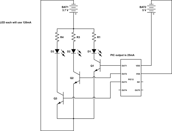
This is a conceptual schema utilizing a PIC12 microcontroller to control the blinking of three LEDs, each exhibiting different blinking patterns. There are several questions that need to be addressed. The circuit design involves a PIC12 microcontroller, which is a...
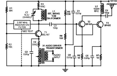
The circuit presented here is a powerful AM transmitter utilizing a ceramic resonator/filter operating at 3.587 MHz. This circuit primarily relies on a transistor for its core functionality. It is possible to use resonators/filters of other frequencies, such as...

220V mains electricity is sent through a 0.33 µF capacitor (Ci) and a 50 kΩ resistive drop. A bridge rectifier composed of diodes D1 to D4 converts the AC voltage to DC. After passing through a 100 µF capacitor...

The R-C twin-tee passive circuit provides band-reject (notch) filtering suitable for portable applications. It has a loaded circuit Q of 0.25. Effective rejection is achievable when the bridge is balanced, which requires close tolerances of the adjustable components, and...
Expanding schematic circuit for the secondary circuit of high-voltage lines. The schematic circuit for the secondary circuit of high-voltage lines is designed to enhance the distribution and management of electrical power in high-voltage systems. This circuit typically includes components...

A straightforward smoke detector circuit has been presented through a schematic diagram, which can be easily constructed and installed in an area for essential detection purposes. The circuit utilizes the versatile FIGARO TGS 813 gas sensor as the primary...