
Delay circuit of a multi-level output

The multi-stage delay circuit utilizes a series of operational amplifiers configured as comparators to achieve precise timing control. Each operational amplifier in the sequence (A1, A2, A3, A4) is designed to respond to the voltage levels at its inverting input. The circuit's functionality is based on the principle that as the voltage at the inverting input (VC1) increases, the output of the operational amplifiers transitions from a high state to a low state, effectively creating a delay.
The voltage divider network connected to the inverting inputs of the operational amplifiers serves to scale down the input voltage, allowing for controlled switching thresholds. The exponential rise of VC1 is critical for defining the timing characteristics of the circuit. The time intervals t1, t2, and t3 correspond to the specific delay settings for each operational amplifier stage, ensuring that the output signals (VA1, VA2, VA3) are generated with the desired timing accuracy.
The dual power supply configuration is essential for the proper operation of the circuit. The positive supplies (+ VE and + VB) provide the necessary voltage levels for the operational amplifiers to function effectively, while the negative supply (-VB) ensures that the output can swing below ground level, which is often required in comparator applications. This arrangement enhances the versatility of the circuit, allowing it to be used in various timing and control applications in electronic systems. As shown having a multi-stage delay circuit is output. The operational amplifier circuit used as comparators, operational amplifier A1 when the applied voltage-inverting input + VE, the operational amplifier A2, A3, A4-inverting input terminal voltage VC1 on the rise along an exponential curve rule. Inverting input of the operational amplifier a voltage is provided by a voltage divider classification.
Therefore, each op amp input Vc1 from zero to + VB (power supply voltage) of t1, t2, t3 time, so that the output signals are inverted, enabling VA1, VA2, VA3 gradual delay purposes. Note that this circuit uses a dual power, namely the positive supply + VE, + VB and the negative supply -VB.
Related Circuits

This is a DC motor controller circuit built using the TIP31 transistor based on the H-Bridge concept. The switches S1 and S2 are normally open, push-to-close buttons. The LED serves to indicate the direction of motor rotation and any...
.png)
This document describes a simple engineering project circuit for a mobile cell phone detector (sniffer). This compact mobile communication detector can sense the presence of a mobile device, making it suitable for preventing mobile phone usage in private spaces,...
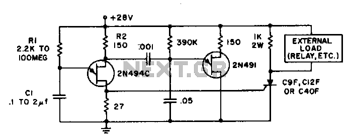
Time delays ranging from 0 milliseconds to over three minutes can be achieved with this circuit without the need for tantalum or electrolytic capacitors. The timing interval begins when power is applied to the circuit. At the conclusion of...
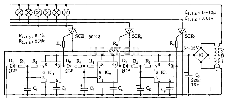
The circuit utilizes a 555 timer as its core component to control three lights through a cyclic trigger monostable delay circuit. The brightest light is controlled by a silicon-controlled rectifier (SCR) that determines the cycle of illumination. When pin...
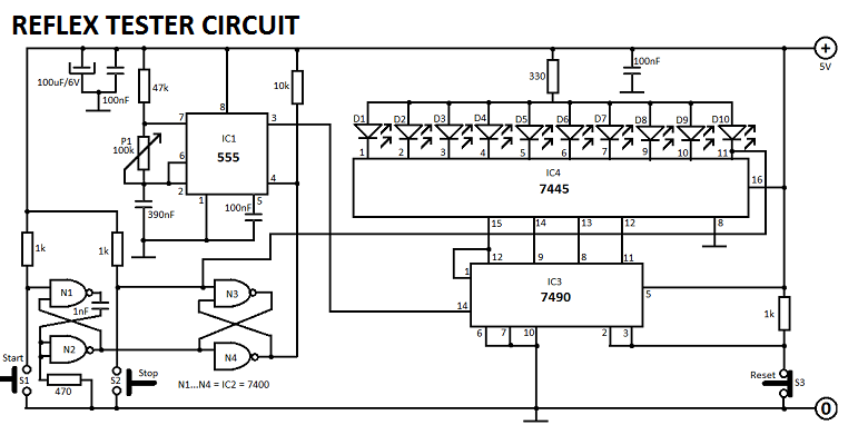
The concept for this crystal tester circuit originated from the necessity to evaluate a large quantity of oscillator crystals that were not in use within a hobby box. Testing each crystal individually without the proper equipment would have been...
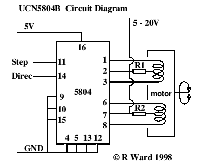
This integrated circuit is highly efficient and does not require any external glue logic for operation. It features two pins to control a motor: one for direction and the other for stepping pulse triggers. The design is compact and...