
Delay switching for power amplifiers

The described delay circuit is primarily utilized in power amplifiers to safeguard against fuse failure during power-up conditions. The core component of this circuit is a relay, which is activated once the capacitors C2 and C3 reach a sufficient charge level. This charging process is critical as it ensures that the relay does not engage until the system is ready, thereby preventing any sudden inrush current that could potentially damage the fuses.
The circuit includes several resistors that play a significant role in controlling the charging rate of the capacitors. Resistors R1 and R2, each rated at 470 kOhm, are likely employed to limit the current flowing into the capacitors, thereby controlling the time it takes for them to charge. Resistor R3, with a value of 220 Ohm, may serve a different purpose, possibly providing a discharge path for the capacitors or influencing the relay's activation threshold.
Resistors R4 to R7, each rated at 10 Ohm and 5 Watts, are wire-wound types that could be used for current sensing or as part of a voltage divider network to monitor the relay's operation. The inclusion of these resistors suggests a design that emphasizes reliability and safety, ensuring that the relay operates under the correct conditions.
Capacitors C1, C2, and C3 are essential for the circuit's operation. C1 is a 330 nF capacitor rated for 400 V, classified as X2-type, which indicates it is suitable for AC applications and can handle voltage spikes. The larger capacitors C2 and C3, each rated at 470 µF and 40-63V, store significant charge to facilitate the relay's operation.
The relay, designated as RE1, is rated for 250 Ohm at 24 V and has contact ratings of 1200 V / 8 A. This indicates that the relay is robust and can handle substantial loads, making it suitable for high-power applications typical in amplifiers.
The fuse, labeled as F1, should be selected based on the specific requirements of the circuit and the power amplifier being used. It is essential to choose a fuse that matches the expected current draw to prevent nuisance blowing while ensuring protection against overload conditions.
Overall, this delay circuit is designed with careful consideration of component ratings and functions, emphasizing safety and reliability in the operation of power amplifiers. Proper attention to the specifications of each component is crucial for the successful implementation of this circuit.This delay can be used in power amplifiers, to prevent the fuses fail when the amplifier is turned on. The circuit is very simple with a relay which turned on when C2 and C3 are charged. If the relay has not been applied, the resistors used to control connected to feed. If after some time the relay attracts the bridge resistors. Watch out for your own safety when building this circuit. On the whole circuit is power. F1 should be the value of having the fuse that normally would be used. R1, R2 = 470 kOhm R3 = 220 ? R4-R7 = 10 ? / 5 W wirewound C1 = 330 nF 400 V ~ X2-type C2-C3 = 470 uF 40 - 63V B1 = B250C1500 RE1 = 250 ? 24 V 1200 V / 8 A Contacts F1 = see text 🔗 External reference
Related Circuits

Figure 1-30 illustrates an example of an output capacitor-less (OCL) power amplifier circuit, which can be analyzed as follows: In this circuit, transistors VTi and VTz form a single-ended input and a differential input single-ended output amplifier configuration. The...
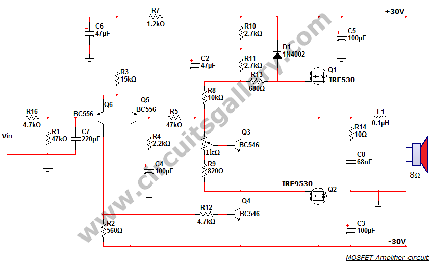
This is a MOSFET transistor-based power amplifier circuit that operates within a voltage range of +35V to -35V. The input voltage is pre-filtered and pre-amplified before being applied to the MOSFET switch. The pre-audio amplifier consists of a differential...
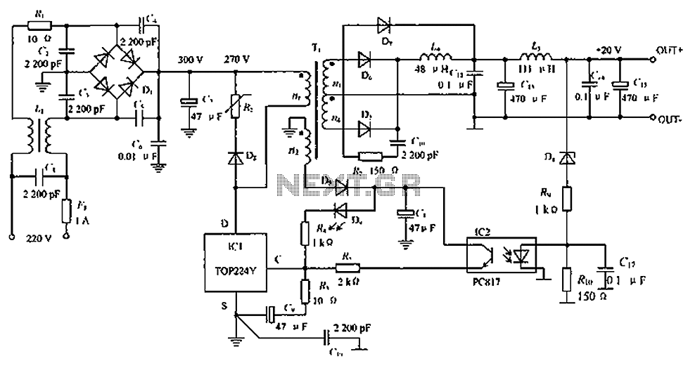
The circuit depicted in the figure is designed to achieve a higher power output by modifying specific components. On the left side of the figure, components R1, L1, D1, and capacitors C1 to C7 form a conventional filtering and...
Up to 10 A continuous output current, or operation with 50 % ESD and 18 A peak current are possible without a fan if sufficient natural air flow is present and the ambient temperature does not exceed 30 °C....
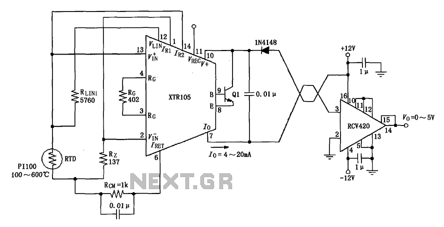
The circuit utilizes a Pt100 type resistance temperature detector (RTD). It operates within a temperature range of 100 to 600 °C, where the XTR105 outputs a current of 4 to 20 mA, and the RCV420 provides an output voltage...

The first schematic is designed for individuals who exclusively purchase electronic components from Radio Shack. It allows for a straightforward shopping experience, enabling one to acquire all necessary parts in-store. For the heat sink, it is recommended to visit...