
Digital counter demonstration circuit

The circuit operates by employing the 555 timer in astable mode to generate a continuous square wave signal. This signal serves as the clock input for the RS7490, which is a binary-coded decimal (BCD) counter. The RS7490 counts from 0 to 9 and outputs the corresponding BCD values. These outputs can then be connected to a 7-segment LED display, allowing for the visual representation of the counted value.
The frequency of the clock signal generated by the 555 timer is determined by the resistor R1, along with another resistor R2 and a capacitor C1, which are part of the timing network. The relationship between these components can be expressed by the formula for the frequency (f) of the output signal:
f = 1.44 / ((R1 + 2R2) * C1)
By adjusting R1, the frequency can be varied, thus controlling the speed at which the RS7490 counts. A lower resistance value for R1 results in a higher frequency, causing the counter to increment more rapidly, while a higher resistance slows down the counting process.
The RS7490 outputs four bits, which represent the decimal values from 0 to 9 in BCD format. Each output pin corresponds to a specific bit in the BCD representation. For instance, when the counter reaches the value '5', the outputs will reflect the binary combination of '0101'. These outputs can be directly connected to the segments of the 7-segment display, which will light up the appropriate segments to display the corresponding decimal digit.
In summary, the combination of the 555 timer and the RS7490 enables the creation of a simple yet effective digital clock circuit that can be visually monitored through a 7-segment display. The ability to adjust R1 provides flexibility in the clock frequency, allowing for customization of the counting speed.555 timer is used as clock to drive RS7490 decimal timer, BCD output to 7 section LED. To adjust R1 can change the clock frequency.. 🔗 External reference
Related Circuits
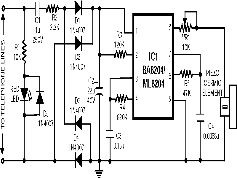
Often, there is a need for an additional telephone ringer in an adjacent room to indicate an incoming call. For instance, if the telephone is located in the drawing room, an extra ringer may be required in the bedroom....
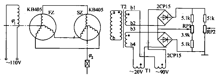
The transmitter (FZ) winding and receiver (SZ) correspond to the three-phase windings connected to a 110V AC voltage supply for transmission. The field winding, early start angle, and receiver output voltage at both ends of the stator windings reflect...

Transistors T1 and T2 form the microphone preamplifier. Resistor R1 provides the necessary bias for the microphone condenser, while preset VR1 functions as a gain control to adjust the gain level. To enhance audio power, the low-level audio output...

Connect the diode VD under test to sockets X1 and X2. A stabilized power supply applies reverse breakdown voltage to VD, allowing the stabilized voltage value Uz to be read from voltage meter V. The stable operating current value...
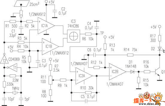
The human approach detector circuit consists of an integrated operational amplifier, a gate circuit, and a resistor-capacitor unit as illustrated in the diagram. The 1 MHz oscillator is composed of a reverser T1, a 1 MHz crystal oscillator, and...
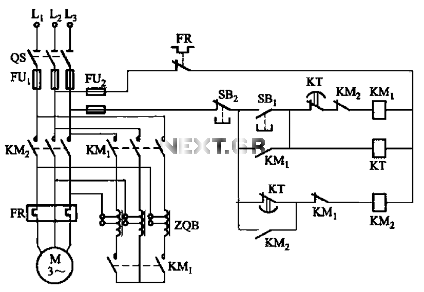
The circuit depicted in Figure 3-49 illustrates an autotransformer that is controlled by a time relay (KT). The delay time set by the KT relay corresponds to the motor's startup duration. The circuit utilizes an autotransformer, which is a type...