
Dual 8051S Execute In Lock-Step

The described circuit functions as a synchronization mechanism for two integrated circuits (ICs), ensuring that they operate in unison by removing clock signals from the slave device until synchronization is achieved. The firmware loop plays a crucial role in generating a WR signal for each iteration, which is essential for monitoring the operational status of both ICs.
The exclusive-OR gate serves as a critical component, comparing the WR signals from both ICs. When there is a discrepancy between the two signals, the exclusive-OR gate outputs a miss-compare pulse. This pulse is vital as it triggers the JK flip-flops, which are designed to latch the state of the synchronization process. The outputs LOCKSTP1 and LOCKSTP2 indicate whether the ICs are in lock-step operation, which is characterized by both circuits executing their programs in sync.
In practical implementations using discrete components, it is recommended to connect to the Q output of the JK flip-flops. This approach simplifies the design by removing unnecessary inverters, thereby enhancing circuit efficiency. The use of ports 1 and 3 of the ICs for this configuration is strategic, ensuring that the necessary signals are accessible for proper synchronization.
It is important to note that utilizing a memory-mapped location for the lock-step-detect clear (K input) is not feasible due to the risk of generating additional WR signals, which could disrupt the synchronization process. Instead, employing the RD signals from the ICs can provide a more effective means of managing the lock-step-detect clear without interfering with the synchronization inputs, thus maintaining the integrity of the synchronization process. This design can be extended to other types of circuits, offering versatility in synchronization applications across various electronic systems. This hardware-software combination deletes clocks from the slave until both /iPs synchronize. The firmware loop causes each to generate a WR signal once per loop. The circuit exclusive-ORs the two WR signals to produce a miss-compare pulse. The miss-compare pulse latches into the two JK flip-flops via outputs LOCKSTP1 and LOCKSTP2. A high on these signals indicates that the /tPs are in lock-step, causing both juPs" programs" execution to exit the firmware loop. If you use discrete components, you"ll probably want to use the Q output of the JK flip-flop and delete the circuit"s inverters.
The listing uses the /iPs" ports 1 and 3. You cannot use a memory-mapped location for the lock-step-detect clear (K input) because this scheme would generate additional WR signals. You could apply this idea to other, perhaps using their RD signals. This way, generating an RD signal to activate the lock-step-detect clear would not affect the synchronization inputs.
Related Circuits
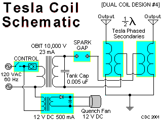
This area illustrates the construction and testing of a new half-wave (dual) Tesla coil. This type of coil features two secondaries driven by a single tank circuit. The design presented is a small and relatively inefficient dual coil constructed...
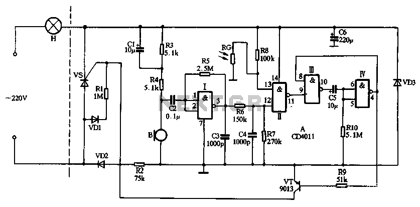
The circuit utilizes CD4011 digital circuits to create a sound-activated light lamp with a dual-control delay section. The left portion of the circuit represents the lighting lines, while the right part consists of the sound and light control delay...
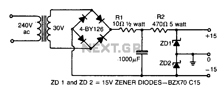
This simple circuit provides both a positive and negative supply from a single transformer winding and a full-wave bridge rectifier. Two zener diodes connected in series create a voltage division, with their junction point grounded. It is important to...
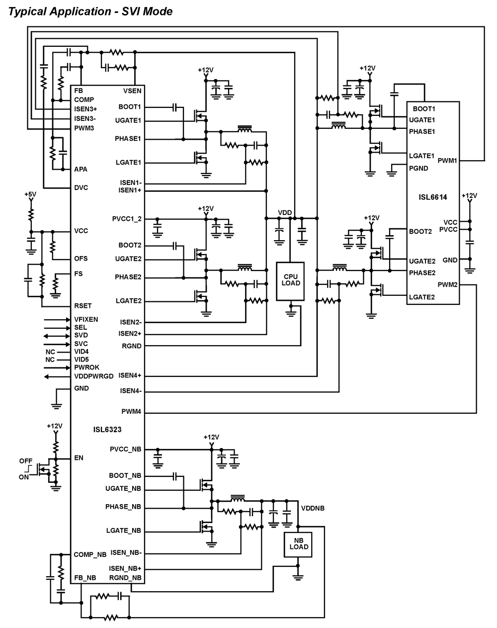
The ISL6323 dual PWM controller provides high efficiency and precise regulation through two synchronous buck DC/DC converters. It supports hybrid power control for AMD processors, operating via either a 6-bit parallel VID interface (PVI) or a serial VID interface...
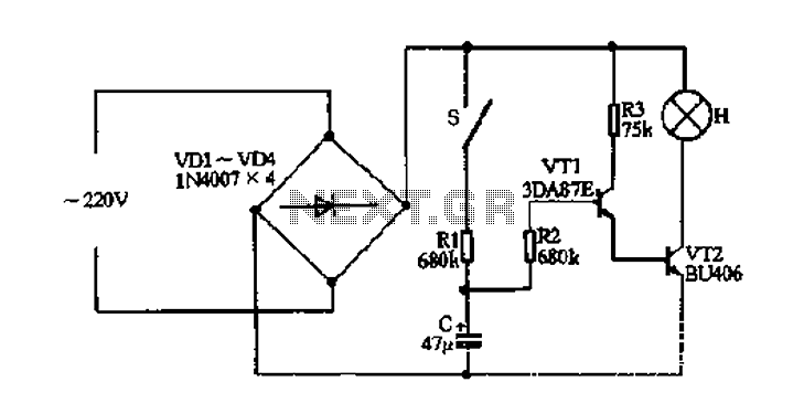
The fade circuit controls the lighting switch depicted in Figure 1-12. The figure illustrates the light switch S, H, which is responsible for lighting. Transistors VT1 and VT2, along with RC components, comprise the fade dimming control circuit. Given...
The UTC A6966 is designed for driving a 5 LED level meter and comes in a 9-lead SIP package. It includes one input amplifier and five comparators for LED level indication. Manufactured by LianShun Electronics Co., Ltd. The UTC A6966...