
Flashing Brake Light Circuit

With the trigger low, the output of U1 is forced high, disabling the triggering of U2. As the triggering is inhibited, the output of U2 switches to a low state, causing Q1 to conduct and turn on the light until the brakes are released. Removing power from the circuits resets SCR1; however, the RC network consisting of R4 and C1 will not discharge immediately, which can trigger SCR1 earlier. Therefore, frequent use of the brakes results in fewer flashes. It is important to note that the voltage drop across the collector/emitter of Q1, along with the losses across the series-fed diodes, reduces the maximum available light output. If the electrical system operates correctly (between 13 to 14 V for most vehicles), these losses will be negligible.
The described circuit operates as a light-flashing system, typically used in automotive applications to indicate braking. The initial activation of Q1 by the low output from U2 ensures that the light is turned on immediately upon power application. The timing function of U1 is crucial, as it establishes the duration and frequency of the flashing light, which is influenced by the values of resistors R8, R6, and capacitor C3. The oscillation of U2, once initiated, continues until SCR1 is triggered, indicating a change in the state of the circuit.
The RC timing network formed by R4 and C1 plays a significant role in controlling the discharge rate, which directly affects how quickly SCR1 can be reset. This is particularly relevant in scenarios where the brakes are applied frequently, as it leads to a quicker re-triggering of SCR1, resulting in fewer flashes of the light. The design must account for the voltage drops across Q1 and the diodes to ensure adequate light output. The circuit is designed to function effectively within the standard operating voltage range of automotive electrical systems, ensuring that the light output remains consistent and reliable under normal conditions. When power is first applied, three things happen: the light-driving transistor (Ql) is switched on because of a low output from U2, pin 3; timer Ul begins its timing cycle, with the output (pin 3) going high, inhibiting U2`s trigger (pin 2) via D2; and charge current begins to move through R3 and R4 to CI.When Ul`s output goes low, the inhibiting bias on U2 pin 2 is removed, so U2 begins to oscillate, flashing the third light via Ql, at a rate determined by R8, R6, and C3. Oscillation continues until the gate-threshold voltage of SCR1 is reached, causing it to fire and pull Ul`s trigger (pin 2) low.
With its trigger low, Ul`s output is forced high, disabling U2`s triggering. With triggering inhibited, U2`s output switches to a low state, which makes Ql conduct, turning on II until the brakes are released. Removing power from the circuits resets SCR1, but the RC network consisting of R4 and CI will not discharge immediately and will trigger SCR1 earlier.
So, frequent brake use means fewer flashes.Bear in mind that the collector/emitter voltage drop across Ql, along with the loss across the series-fed diodes, reduces the maximum available light output. If the electrical system is functioning properly (at 13 to 14 V for most vehicles), those losses will be negligible.
Related Circuits

Voltage regulator ICs (78xx series) provide a steady output voltage, in contrast to a widely fluctuating input supply, when the common terminal is grounded. The 78xx series of voltage regulator integrated circuits (ICs) are widely utilized in electronic circuits to...

The transistor is configured as an audio oscillator, utilizing an audio transformer in the collector. The secondary winding is connected to a linear potentiometer. The ratio between the two sections of the potentiometer from the slider is proportional to...

This DC voltage doubler circuit generates a voltage that is double its supply voltage. It is beneficial when a higher voltage level is required from a single power source. The DC voltage doubler circuit typically employs a combination of capacitors...
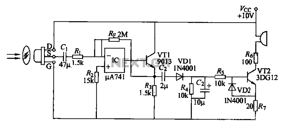
A simple burglar alarm circuit utilizes a pyroelectric sensor (IRA-E100SZI). When human movement is detected, it triggers an electric buzzer alarm. The sensor receives signals through an AC amplifier, which is then converted by a rectifier circuit into a...
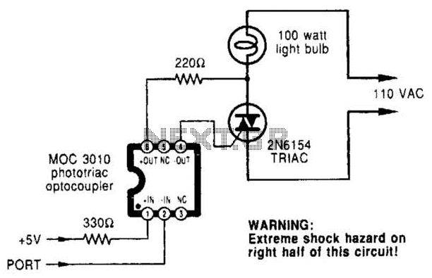
A microcomputer-to-triac interface utilizes a phototriac optoisolator to safely isolate logic signals, allowing direct control of high-power loads. This circuit can function as either an on/off switch or a proportional phase control, depending on the input waveforms and the...

This circuit diagram for a logic tutor kit was created using MS Word graphics. While modern software is commonly utilized, there may be instances where traditional methods are necessary. Employ a sharp pencil and a ruler to ensure precision;...