
fm antenna booster circuit

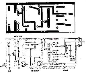
The FM antenna booster circuit is designed to amplify weak radio frequency signals received from distant FM stations, improving audio clarity and reception quality. The core component, the 2SC2570 transistor, operates as a common-emitter amplifier, providing significant gain to the incoming RF signals. This transistor is suitable for VHF/UHF applications, making it ideal for FM reception.
The circuit layout should prioritize minimizing interference and ensuring stable operation. The use of a high-quality printed circuit board (PCB) is essential to reduce parasitic capacitance and inductance, which can adversely affect performance. The input and output trimmers (VC1 and VC2) allow for fine-tuning of the circuit to achieve maximum gain, accommodating variations in signal strength and frequency.
Coil L1, with its four turns of 20 SWG enameled copper wire, serves as the input inductor, which is crucial for tuning the circuit to the desired frequency. The spacing of the windings is important for maintaining the coil's inductance and minimizing losses. The tap on L1 enables the circuit to adjust its input impedance, optimizing the signal transfer from the antenna to the amplifier. Coil L2, with three turns, acts as a coupling inductor, further enhancing the signal amplification process.
The pin configuration of the 2SC2570 transistor should be carefully followed to ensure proper connections and functionality. The circuit may also benefit from additional components such as bypass capacitors to stabilize the power supply and improve overall performance. Proper grounding techniques should be employed to minimize noise and improve signal integrity.
In summary, the FM antenna booster circuit is a straightforward yet effective solution for enhancing FM signal reception, making it an excellent project for electronics enthusiasts and professionals alike.This is a low cost fm antenna booster that can be used to listen to program from distant FM stations clearly. The antenna fm booster circuit comprises a common-emitter tuned RF preamplifier wired around VHF/UHF transistor 2SC2570 (C2570).
This is the schematic of the simple FM Antenna Booster. Assemble the circuit on a good quality of printed circ uit board. Adjust input/output trimmers (VC1/VC2) for maximum gain. Input coil L1 consists of four turns of 20SWG enameled copper wire (slightly space wound) over 5mm diameter former. It is tapped at the first turn from ground lead side. Coil L2 is similar to L1, but has only three turns. Pin configuration of transistor 2SC2570 is shown in the fm antenna booster schematic. 🔗 External reference
Related Circuits
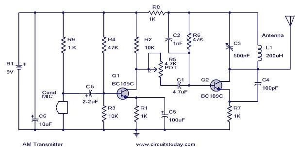
This document presents a circuit diagram of a simple AM transmitter that is capable of transmitting audio signals to a specified area. The circuit is designed with a limited power output to comply with FCC regulations while effectively producing...
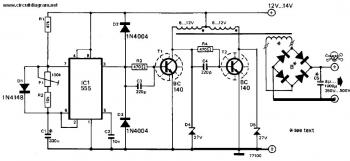
This inverter circuit is designed to power electric razors, stroboscopes, flash tubes, and small fluorescent lamps using a 12-volt car battery. Unlike typical feedback oscillator inverters, this design features a separate oscillator from the output stage, allowing for easy...
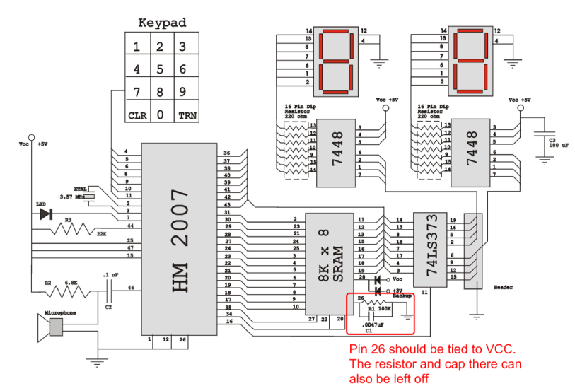
Verify the pin configurations on the datasheets for the integrated circuits used in your project, making necessary adjustments. In this instance, the RAM chip utilized had a non-inverted enable signal on pin 26, while the schematic assumed it was...
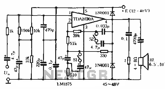
This circuit features bass boost compensation for a practical power amplifier. It is important to adhere to the specified parameters of the amplifier circuit elements. When switches S1 and S2 are disconnected, the bass boost function can be set...
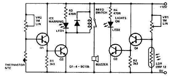
This electronic project circuit diagram for an ice warning and lights reminder system alerts drivers when their vehicle lights should be activated and warns them if the outside temperature approaches zero degrees Celsius. The system employs an LED indicator...
The system primarily consists of a permanent magnet disk, an integrated Hall sensor, a strobe gate, time base signal circuits, a power counting circuit, and a digital display circuit. The counting and digital display circuit utilizes the CMOS-LED digital...