
Inverter 12V DC to 240V DC circuit diagram

This inverter circuit operates efficiently by utilizing a 555 timer as the core oscillator, configured in an astable mode to generate a continuous square wave signal. The frequency of this signal can be adjusted by varying the resistor and capacitor values connected to the 555 timer, enabling flexibility for different load requirements. The square wave output drives the base of the first transistor (T1), which acts as a switch, allowing current to flow through one half of the transformer’s primary winding. This switching action is crucial for creating the alternating magnetic field necessary for inducing voltage in the secondary winding.
The second transistor (T2) complements T1 by switching current through the other half of the primary winding during the opposite phase of the input signal. This complementary operation ensures that the transformer is effectively utilized, maximizing energy transfer and improving efficiency. The use of Zener diodes D4 and D5 provides essential protection against voltage spikes, which can occur due to the inductive kickback when the transistors switch off. This protection mechanism is vital for maintaining the integrity of the transistors and ensuring long-term reliability of the inverter circuit.
The transformer itself is a critical component, as it steps up the voltage from the primary to the secondary winding. The turns ratio of the transformer determines the output voltage level, which can be tailored to meet the specific requirements of the connected devices. Depending on the application, the output from the secondary winding may either be used directly or passed through a rectifier circuit to convert the AC voltage to DC, suitable for devices that require a stable DC input. This inverter circuit's design is versatile, making it suitable for a range of applications where portable or battery-operated power sources are necessary.This inverter circuit can be used to power electric razors, stroboscopes and flash tubes, and small fluorescent lamps from a 12 volt car battery. In contrast to the usual feedback oscillator type of inverter, the oscillator of this inverter is separate from the output stage, which allows easy adjustment of the oscillator frequency to suit differen
t applications. The oscillator circuit consists of a 555 timer connected as an astable multivibrator. The inclusion of D1 ensures that the duty-cycle of the squarewave output is maintained at about 50%. The output of the 555 drives the base of T1 which switches current through one half of the primary of the transformer. T2 is driven from the collector of Tl and thus switches current through the other half of the transformer winding on opposite half cycles of the drive waveform.
Zener diodes D4 and D5 protect Tl and T2 from any high-voltage spikes generated by the transformer. The voltage applied to the transformer primary is stepped up and the required high output voltage appears across the secondary winding. Depending on the application the secondary voltage may or may not be rectified. 🔗 External reference
Related Circuits
After being careful about every orientation of every transistor, a circuit board was designed around the LM387N, which was not the intended chip nor the one originally ordered (LM258, commonly referred to as LM358). During testing before adding larger...

Illuminate your tabletop with this stylish White LED Lamp. It is powered through a USB port, making it perfect for taking notes while browsing the internet. The USB port can provide a convenient power source. The White LED Lamp is...
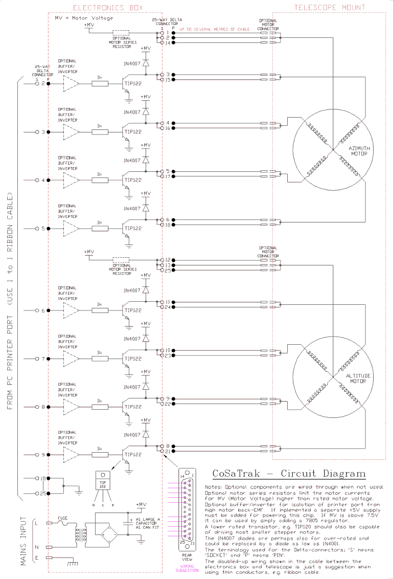
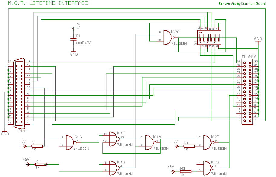
The back EMF voltage spikes produced by stepper motors, especially higher voltage motors, can damage a PC's printer port if connections are made incorrectly, flyback diodes are absent, or connected in reverse. The safest options are opto-isolated or buffered/inverted...
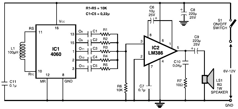
The circuit is built around the popular CMOS oscillator-divider IC 4060 and a small audio amplifier LM386. The IC 4060 functions as a multitone generator. A 100 H inductor is used at the input of the IC 4060, allowing...
Section Ul-a is configured as a high-gain inverting voltage amplifier that is inductively coupled to the phone line via LI. Inductor LI is a homemade unit that consists of 250 turns of fine, enamel-coated wire that is wound on...
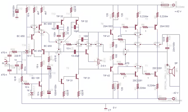
This post presents the circuit schematic diagram for a 500-watt mono power amplifier. As of July 18, 2012, the intention is to create a power sound system with a total output of 1000 watts in stereo. The design utilizes...