
Frequency comparator circuit

The circuit utilizes a gating mechanism wherein Input 1 establishes a time window for valid signal detection from Input 2. The logic state of Input 2 is pivotal; a single rising edge during the gating period triggers a transition to a logic 1 output, while any other frequencies during this timeframe lead to a logic 0 output. This function is facilitated by IC1a, which processes Input 1 into a narrow pulse signal. This pulse serves as an initialization signal for IC2, which is configured as a two-stage shift register. The clocking of this shift register is directly influenced by Input 2. On the initial rising edge of Input 2, IC2b outputs a logic 1, indicating the detection of the valid signal, while all subsequent edges result in a logic 0 output, effectively creating a one-shot response to the first edge.
The output from IC2b is then latched by IC3 at the end of the gating period, establishing a lock output that signifies the successful capture of the input signal. To ensure that this output can be monitored visually, a monostable multivibrator is employed. This component generates a temporary pulse that can be observed, thus allowing for real-time monitoring of the system's state. The design allows for flexibility in output selection, enabling the user to choose between two outputs from IC3 based on the importance of the respective states. The current configuration is particularly useful for indicating a failure state, providing critical feedback for system diagnostics.Input 1 is used as a gating period, during which a single rising edge on input 2 will cause a logic 1 output-any other number, indicating non-identical frequencies causes a logic 0 output. ICla converts input 1 to a narrow pulse which initializes IC2 which forms a two-stage shift register clocked by input 2.
On the first edge of input 2 a logic 1 appears on the output of IC2b and for all subsequent inputs a logic 0 is present. At the end of the gating period this output is latched by IC3 forming the lock output. As this is only valid for one input period a monostable is added to the output to enable, for example, visual monitoring of the output. Either output from IC3 can be used depending on which state is most important. As connected the failure state is indicated.
Related Circuits
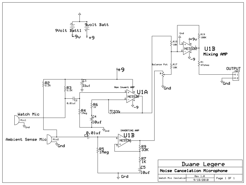
A microphone is designed to listen to a wristwatch while canceling ambient noise in the room. A circuit has been included, which is based on a headphone cancellation circuit. The schematic will be provided shortly. The suggested approach is...
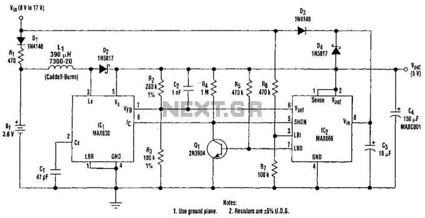
A 9-V wall adapter supplies Vm. IC2 contains a low-battery detector circuit that senses l7IN through resistors R6 and R7. The detector output at pin 7 drives an inverter (Q1), which in turn controls the shutdown inputs of IC1...
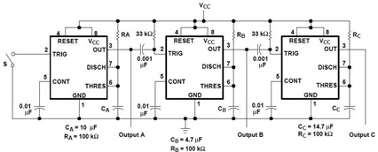
A sequential timer circuit device is utilized in various applications for initializing conditions during start-up or for activating test signals in sequences, such as in test equipment devices. The circuit diagram below illustrates a sequencer circuit with potential applications...
If a complete circuit is needed, there are thousands of these circuits available in the designs. Some of them can be provided easily, but further communication is required. The request indicates a need for a comprehensive circuit design, which may...

The 78W series voltage regulators are designed to handle an input voltage of approximately 35V, while the 24V type can withstand up to 40V. It should be noted that these regulators will not operate effectively with a significant input-output...
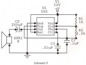
This circuit features an astable oscillator constructed around a 555 timer, generating an alarm tone of 1.8 kHz, which directly drives a speaker. It serves as a fundamental alarm circuit that can be utilized in various projects. Although the...