
Frequency doubler II

The described frequency doubler circuit utilizes a CMOS quad two-input NAND gate IC, specifically the 4011 package, to achieve frequency multiplication. The core operation relies on the conversion of an input frequency to its double by employing a combination of logic gates and differentiating networks.
The circuit is structured around an inverter (IC1B) that is responsible for inverting the input signal. This inversion is crucial as it helps to create the necessary phase shifts required for the frequency doubling process. The differentiating networks, composed of resistors (R1, R2) and capacitors (C1, C2), play a significant role in shaping the input waveform. These networks convert the square wave input into a series of sharp pulses, which are essential for effective triggering of the NAND gates.
The NAND gates (IC1A, IC1C, and IC1D) serve multiple functions in this circuit. IC1A acts as the primary logic gate to process the differentiated signals, while IC1C and IC1D are utilized as buffers to ensure that the output signals maintain their integrity and drive capabilities. This arrangement allows for a robust output that can effectively double the frequency of the input signal.
The output of the circuit presents a waveform that oscillates at twice the frequency of the original input, demonstrating the effectiveness of the frequency doubler. The arrangement of components ensures minimal signal degradation, allowing for a clean and precise output waveform. The use of CMOS technology contributes to low power consumption and high-speed operation, making this frequency doubler suitable for various applications in signal processing and communication systems.
In summary, the frequency doubler circuit based on the CMOS quad NAND gate 4011 is a well-structured design that efficiently converts an input frequency into its double using inverting and buffering techniques, along with differentiating networks for optimal signal shaping. This frequency doubler uses one CMOS quad, two input NAND gate package type 4011. The frequency doubler proper consists of an inverter IC1B, two differentiating networks R1/C1, R2/C2 and NAND gate IC1A, IC1C and IC1D function as input and output buffers. In Fig.2 exist the pulses in different points of circuit. 🔗 External reference
Related Circuits
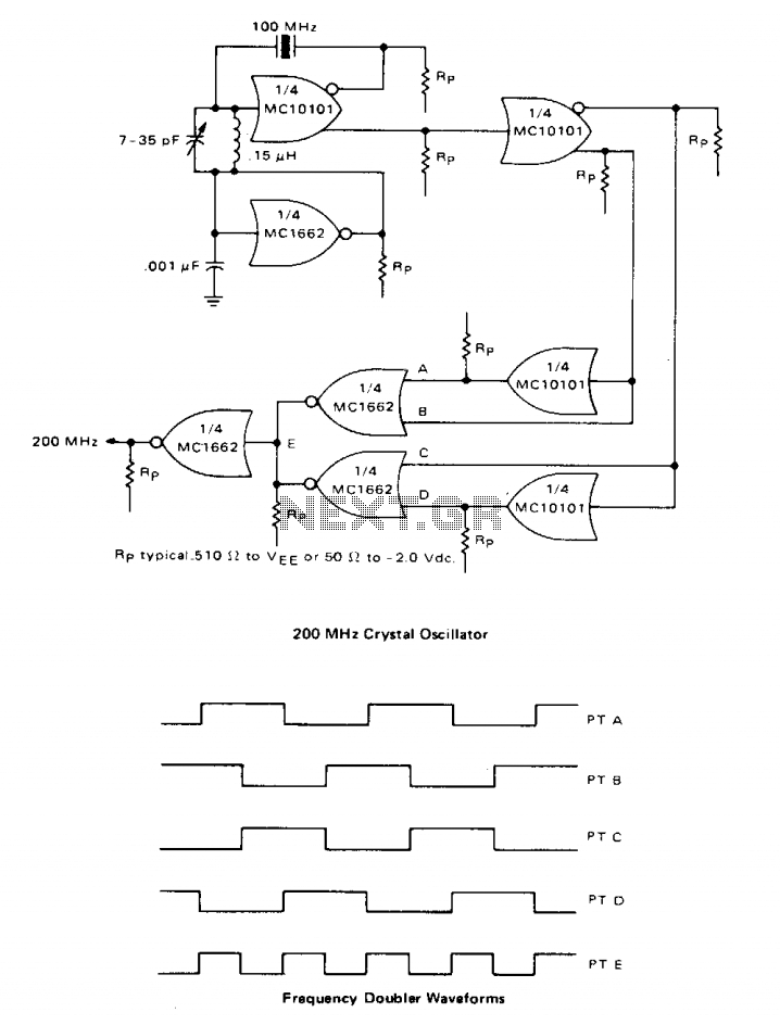
A high-speed oscillator can be created by integrating an MECL 10 crystal oscillator with an MECL III frequency doubler. One section of the MC10101 is configured as a 100 MHz crystal oscillator, with the crystal placed in series within...
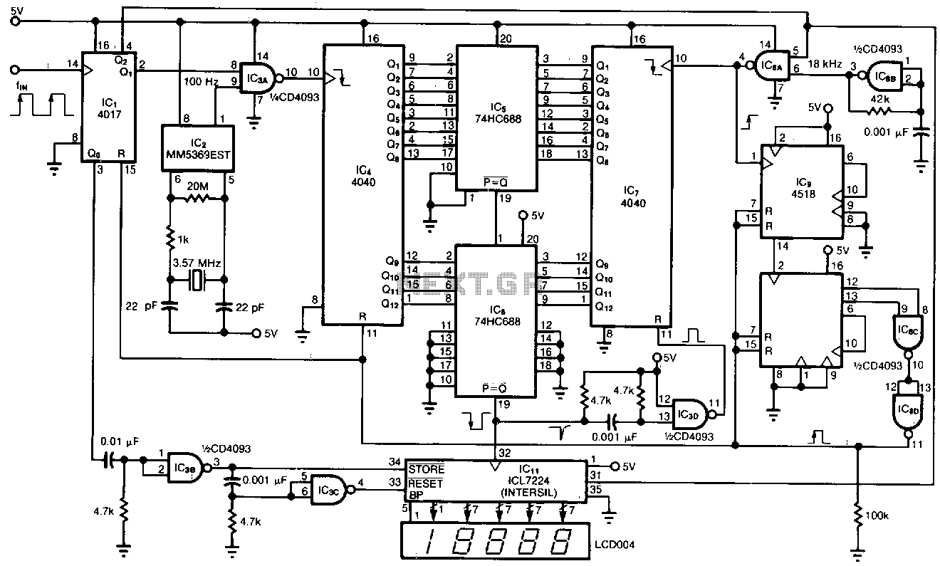
This tachometer allows for the measurement of heartbeats, respiratory rates, and other low-frequency events that occur at intervals ranging from 0.33 to 40.96 seconds. The circuit detects the frequency, calculates the corresponding pulses per minute, and updates the LCD...
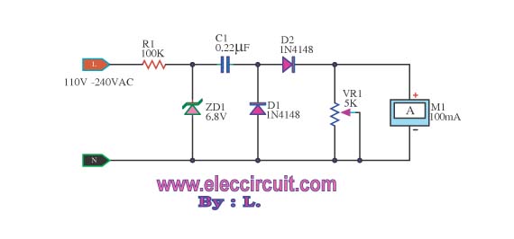
This meter displays the frequency of a power generator, which operates at a voltage range of 110V-240V and a frequency range of 10-100Hz. The output sine waves are converted to square waves. The described frequency meter is designed to accurately...
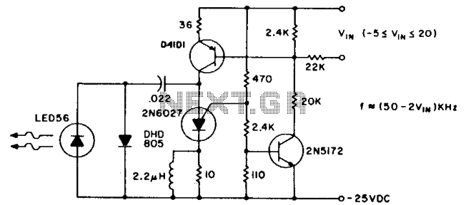
The pulse repetition rate is largely unaffected by temperature and power supply voltage, and it varies linearly with V1N, the modulating voltage. Effective information transfer was achieved at distances of 12 feet (~4m) in free air. A greater range...
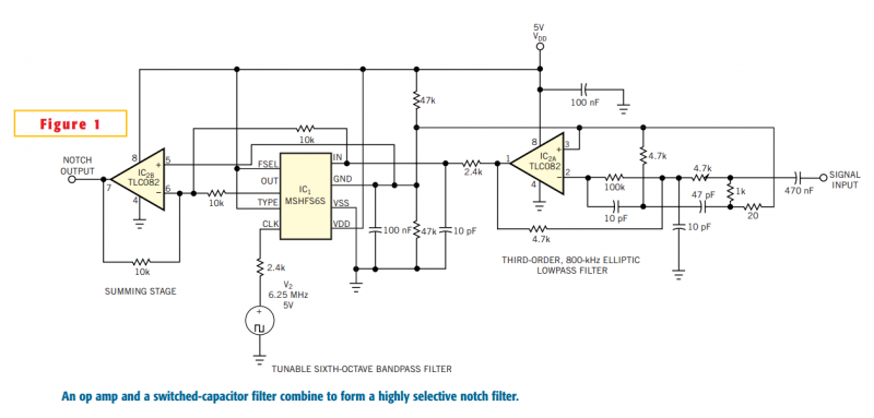
Although you can obtain universal, resistor-programmable switched-capacitor filters that are configurable as notch filters, most cannot operate at bandwidths higher than 100 kHz. Further, the typically 16- to 20-pin packages do not include a continuous-time, antialiasing filter to prevent...
The circuit utilizes a 555 timer configured as a multivibrator, where the oscillation frequency is determined by resistors R1, R2, and capacitor C1. The frequency formula is given by fo = 1.443 / ((R1 + R2) * C1). The...