
Function Generator 2

In practical design, adjustments can be made to the linearizing resistors R32 and R33, which can be reduced from 120 ohms to 12 ohms. This modification may lead to clipping in the output waveform. Conversely, increasing R32 and R33 to 240 ohms can result in a more linear gain, causing the output to resemble the triangle wave. The output scaling can be manipulated by adjusting R42 and R44, which can be increased or decreased by a factor of two.
The circuit includes a frequency control section powered by a DC voltage source (VS) and a sine wave generator. The inverter stage consists of resistors R3 and R4, along with an operational amplifier (XOP2). An integrator section is formed by resistors R1 and R2, with a switch (S1) included to control signal flow. Threshold components (RTH1 to RTH4) and comparators (XCMP1 and XCMP2) are integrated to manage signal processing. The design utilizes flip-flops (XNAND1, XNAND2) for logic operations and incorporates power supplies for the logic gates and thresholds.
The sine shaping is achieved through a differential amplifier configuration involving resistors R30 and R31, and transistors Q30 and Q31. The resistors R32 and R33 are critical in controlling the linearity of the output waveform. The current-to-voltage converter section consists of resistors R41, R42, R43, and R44, with an operational amplifier (XOP3) used for signal conditioning.
This comprehensive circuit design effectively demonstrates the transformation of a triangle wave into a sine wave through careful manipulation of resistive components and operational amplifiers, showcasing the principles of analog signal processing in function generator applications.How to take the triangle wave waveform and bend it into a sine wave. To help adjust its transfer function, resistors R32 and R33 are added. Increasing or decreasing these resistors causes the response to be more or less linear. How do we take our differential output current from the the Q1, Q2 pair above and convert it back to voltage Here`s a handy circuit that`s easier to analyze than it looks. The transistor outputs are modeled as current sources. Although the transistors do have an output impedance across current sources, the value is typically so high where it won`t significantly affect circuit operation. Let`s see how this circuit works. Notice R30 and R31 attenuate the signal by ~10x so that the differential pair is not over driven with too large of an input.
Choosing R34=5k sets up about 0. 5mA flowing in each transistor. The resistors for the current to voltage converter were initially chosen as R41, 42, 43, 43=2k. You can increase R42 and R44 to increase the output. CIRCUIT INSIGHT Run a transient simulation and plot the triangle wave output V(3). In another plot window, add the transistor collector currents IC(Q30) and IC(Q31). Finally go back to the original plot and add the sine wave output at V(36) to see the difference of currents converted back to a voltage. In many classic function generator circuits, this is how the triangle wave becomes a sine wave! HANDS-ON DESIGN Now, let`s monkey with the controls. Reduce linearizing resistors R32, 33 from 120 to just 12 ohms. Rerun the simulation and check out V(36). What happened to the beautiful sine wave. Looks like there`s too much clipping! Try increasing R32, 33 to 240 ohms. What happened to the output V(36). Looks like the gain is too linear where the output starts resembling the triangle wave. Finally, you can scale the output by adjusting R42, 44. Try increasing or decreasing R42, 44 by a factor of 2. Rerun the simulation. Did the output scaled as you expected FUNCTION_GEN. CIR - TRIANGLE, SQUARE, SINE GENERATOR * * FREQUENCY CONTROL VS 1 0 1VDC *VS 1 0 SIN(1V 0. 4VP 100HZ) * INVERTER R3 1 4 10K R4 4 5 10K XOP2 0 4 5 OPAMP1 * INTEGRATOR R1 1 2 10K R2 6 2 5K S1 6 5 15 0 SWA CI 2 3 10NF IC=0V XOP1 0 2 3 OPAMP1 * * THRESHOLDS RTH1 20 22 5K RTH2 22 0 5K RTH3 0 23 5K RTH4 23 21 5K * * COMPARATORS XCMP1 3 22 11 COMP1 XCMP2 23 3 12 COMP1 * * RS FLIP-FLOP XNOT1 11 13 20 NOT XNOT2 12 16 20 NOT XNAND1 13 14 15 20 NAND XNAND2 15 16 14 20 NAND * PWR FOR LOGIC GATES AND THRESHOLDS VCC 20 0 +5V VDD 21 0 -5V * SINE SHAPER - DIFF AMP R30 3 31 10K R31 31 0 1K * Q30 30 31 32 QNPN Q31 34 0 35 QNPN R32 32 33 120 R33 35 33 120 R34 33 21 5K * CURRENT TO VOLTAGE AND LEVEL SHIFTER R41 20 30 2K R42 30 0 2.
5K R43 20 34 2K R44 34 36 2. 5K XOP3 30 34 36 OPAMP1 * * SUBCIRCUITS AND MODELS * *. SUBCKT NAND 1 2 3 4 * TERMINALS A B OUT VCC RL 3 4 500 CL 3 0 10PF S1 3 5 1 0 SW S2 5 0 2 0 SW. ENDS *. SUBCKT NOT 1 3 4 * TERMINALS A OUT VCC RL 3 4 500 CL 3 0 10PF S1 3 0 1 0 SW. ENDS *. SUBCKT COMP1 1 2 5 * TERMINALS: 1-INPUT+, 2-INPUT-, 5-OUTPUT * DIFF AMP WITH HYSTERESIS EDIFF 3 0 VALUE = { V(1) - V(2) + V(5)/1000} * FREQUENCY RESPONSE RP1 3 4 500 CP1 4 0 100PF * LIMITER EOUT 5 0 TABLE {V(4)} = (-5MV 0V) (5MV, 5V). ENDS * * * OPAMP MACRO MODEL, SINGLE-POLE WITH 15V OUTPUT CLAMP * connections: non-inverting input * | inverting input * | | output * | | |.
SUBCKT OPAMP1 1 2 6 * INPUT IMPEDANCE RIN 1 2 10MEG * DC GAIN=100K AND POLE1=100HZ * UNITY GAIN = DCGAIN X POLE1 = 10MHZ EGAIN 3 0 1 2 100K RP1 3 4 100K CP1 4 0 0. 0159UF * OUTPUT BUFFER AND RESISTANCE EBUFFER 5 0 4 0 1 ROUT 5 6 10. ENDS * *. MODEL SWA VSWITCH(VON=2 VOFF=3 RON=1 ROFF=1e6). MODEL SW VSWITCH(VON=3 VOFF=2 RON=10 ROFF=100K). model QNPN NPN(BF=100) * * * ANALYSIS *. T 🔗 External reference
Related Circuits

This circuit is utilized to observe the response of an intermediate frequency (IF) amplifier or a filter. It can be employed with an oscilloscope or, for a broader dynamic range, with a spectrum analyzer. The circuit designed for observing the...
Cuckoo Sound Generator Circuit Schematic. This circuit generates a two-tone effect similar to the cuckoo song. It can be utilized for doorbells or other applications due to a built-in audio amplifier and loudspeaker. The Cuckoo Sound Generator Circuit is designed...
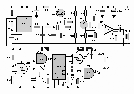
This is a simple triangle-wave generator utilizing two integrated circuit (IC) devices and a transistor. The triangle wave serves as feedback to the square-wave generator. It allows range switching across three intervals from 100 Hz to 100 kHz. Additional...
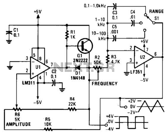
A variable dock-pulse generator consists of two sections of IC1, which is a 4069 CMOS hex inverter, along with resistor R1, switch S1, and capacitors C1 through C6. By adjusting R1 and switching one of the capacitors into the...
A teardown of a BK Precision 4011 5MHz function generator revealed that, like most basic function generators from earlier times, the BK 4011 does not include frequency sweep as a standard option. However, it does feature a VCG (Voltage...
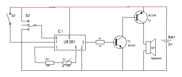
This is a simple audio circuit utilizing the UM3561 for generating melodies that can be employed in toys and various home appliances. It serves as an excellent project for novice beginners. The UM3561 is a dedicated melody generator integrated circuit...