
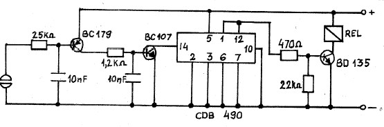
General Hobbyist Circuits

A binary counter is typically implemented using a binary flip-flop, which can be viewed as a toggle switch with two states: ON (binary 1, HIGH) and OFF (binary 0, LOW). A binary flip-flop counter counts in a sequence, such as 0, 1, 0, 1, etc. A basic binary counter can be constructed using one or more flip-flops connected in a way that the binary number stored in these flip-flops represents the total number of trigger pulses received at the counter input.
A ring counter consists of two or more flip-flops connected in series, where the output of one flip-flop serves as the input to the next. In this configuration, all outputs are set to binary 0 except for one flip-flop, which is set to binary 1. Pulsing the input of the ring counter sequentially changes the state of the succeeding flip-flop from 0 to 1, with the flip-flop containing the binary 1 indicating the current count. The maximum number of pulses that can be counted by N flip-flops is equal to N.
A serial entry shift register resembles a ring counter; however, the output flip-flop is not connected to the input flip-flop. The flip-flops are cascaded so that the output from one flip-flop becomes the input of the next. All set trigger and reset trigger inputs are tied together to form a shift bus. Clock pulses applied to the shift bus cause the stored binary information to shift from left to right, one bit position per clock pulse.
In this circuit, a serial input/output with parallel output register has its 5th and 6th bits exclusive ORed to the serial input, forming a pseudo-random sequencer, also known as a pseudo-random number generator. The CMOS logic ICs utilized include one 4070 XOR (Exclusive OR) and three CD4013B D flip-flops. LEDs were employed to observe the binary state of the clock and each of the 6 bits of the shift register. Since only one XOR gate is required for the shift register, the remaining gates were configured to create the clock. These gates are wired as inverters to form an astable multivibrator with a frequency of approximately 0.45 Hertz or 27 pulses per minute.
The clock schematic and pin 1 markings for all digital ICs are illustrated. The output LED, while not mandatory, provides immediate feedback on whether the clock is functioning. The circuit is designed using "Ugly Construction," with the ICs arranged in a "dead bug" fashion. The clock speed can be increased by reducing the value of the 100K resistor or the capacitor values, following the formula for frequency: F Hertz = 1 / (2.2 * R * C), where R is in ohms and C is in farads. The slow clock speed was deliberately chosen to facilitate better observation of the digital output from the shift register.
In the shift register, each CD4013 was configured as two cascaded flip-flops connected to the clock. Power was applied, and a test lead was used to bring pin 5 of the first flip-flop HIGH (connected to 12 volts for 1-2 seconds). Both flip-flop state monitor LEDs illuminated sequentially with subsequent clock pulses. Following this, pin 5 was set LOW (shorted to ground with a test lead for a couple of seconds), causing each LED to turn OFF in sequence with subsequent clock pulses.This circuit describes a simple, 6-bit random number pseudo-generator used to study binary counters and in particular, shift registers. Some very basic background information about binary counters and shift registers is provided. In reality there are dozens of different shift register topologies available and it can get quite complex.
If you wish to find a good logic tutorial website, I strongly recommend Ken Bigelow`s site as it has interactive diagrams. Flip-flops are also covered well on wikipedia and many other web sites. Binary Counter: The circuit most often used as a counter is called a binary flip-flop. The basic flip-flop can be viewed as a toggle switch having either an ON or OFF position. This is the binary state 1 (HIGH) or 0 (LOW). Like the toggle switch, the binary flip-flop has 2 binary states 1 or 0. A binary flip flop counter counts in a sequence such as 0, 1, 0, 1 etc. A straight binary counter can be built by using 1 or more flip-flops connected in a manner that the binary number stored in these flip-flops will represent the total number of trigger pulses received at the counter input.
Ring Counter: A ring counter has 2 or more flip-flops cascaded so that the output from one flip-flop becomes the input of the next flip-flop. The flip-flops are connected so that all of their outputs are at the binary state 0 except for one flip-flop.
By pulsing the input of the ring counter, it will sequentially change the binary state of the succeeding flip-flop from binary 0 to binary 1. The flip-flop that contains the binary 1 indicates the count of this binary counter. The maximum number of pulses that can be counted by N flip-flops is N pulses. Shift Register: A serial entry shift register is similar to a ring counter, except that the output flip-flop is not connected to the input flip-flop.
Like the ring counter, the flip-flops are cascaded so that the output from one flip-flop becomes the input of the next flip-flop. All the set trigger and reset trigger inputs are tied together to form what is called a shift bus. Clock pulses are applied to the shift bus to cause the stored binary information to shift from left to right; one bit position per each received clock pulse.
In Figure 2, this serial input/output + parallel output register has its 5th and 6th bits exclusive ORed to the serial input to form a pseudo-random sequencer, which is called a pseudo-random number generator by some. The CMOS logic ICs used were one 4070 XOR (Exclusive OR) and three CD4013B D flip-flops. Junk box LEDs were used to observe the binary state of the clock and each of the 6 bits of the shift register.
Since only one XOR gate is needed for the shift register, the remaining gates were configured to make the clock. These gates are essentially wired up as inverters to form an astable multivibrator with a frequency of about 0.
45 Hertz or 27 pulses per minute. Shown above in Figure 1 is the clock schematic and the pin 1 marking for all of the digital ICs on this web page. The output LED is not mandatory, but will instantly tell you whether or not your clock is working. I built this whole circuit using Ugly Construction with the ICs flipped upside down in a "dead bug" fashion.
You can increase the clock speed by decreasing the 100K resistor or the capacitor values. F Hertz = 1/ (2. 2 * R * C) with R in ohms and C in farads. The slow clock speed was chosen to better observe the digital output of the shift register. In Figure 2 is the shift register. Each 4013 was wired up as 2 cascaded flip-flops and connected to the clock. Power was applied and then a test lead was used to bring pin 5 of the first flip-flop HIGH (connected to 12 volts for 1-2 seconds). Both flip-flop state monitor LEDS turned ON in sequence with subsequent clock pulses. Afterwards, pin 5 was set LOW (shorted to ground with a test lead for a couple of seconds) and each LED turned OFF in sequence with subsequent clock p
🔗 External reference
Related Circuits
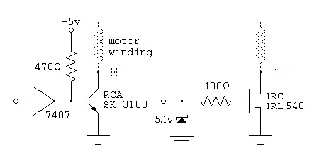
To control a stepper motor, each winding must be energized individually in a specific and timed sequence. This energization is carried out by a driver circuit, which acts as an amplifier. The timing is managed by an indexer circuit,...
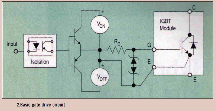
High power IGBT modules utilize hybrid integrated circuit (IC) gate drives that incorporate protection circuits, which implement desaturation detection or real-time control. High power Insulated Gate Bipolar Transistor (IGBT) modules are essential components in various high-efficiency power conversion applications, such...

This circuit provides a DC output to a meter and an audio output (if necessary) for checking transmitters or modulated signals. It can also be used as a field strength meter or transmitter monitor. The circuit is designed to facilitate...
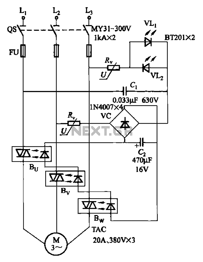
The circuit depicted in Figure 3-93 is integrated with an optical phase sequence protection relay. The circuit in question is designed to provide phase sequence protection using an optical relay mechanism. Optical phase sequence protection relays are crucial in applications...
This is a simple mains power failure alarm circuit that activates an alarm when the mains supply is lost. Unlike many similar circuits, this design does not require a backup power source, such as a battery, to operate the...
A collection of touch switch circuits is presented. A touch switch is an electronic device that allows control of a circuit simply by touching a sensor. The circuit diagram illustrates a simple design that utilizes only eight components. The...