
Generating a Delayed Pulse Using The 555 Timer circuit

The circuit employs two 555 timer ICs configured in monostable mode to achieve the desired pulse generation and delay. The first 555 timer is triggered by a momentary push-button switch, which, when pressed, causes the output to transition high, activating the relay. The output remains high for a predetermined duration, set by an external resistor and capacitor connected to the timing pins of the first 555 timer. This timing component determines the length of the delay before the output transitions back to low.
Once the output of the first timer returns to low after the delay, this falling edge is fed into the trigger pin of the second 555 timer. The second timer is also configured in monostable mode, and it is designed to produce a pulse of a specified width. Its timing components (resistor and capacitor) set the duration of this pulse. The output of the second timer, which drives the relay, remains high for the duration of this pulse, allowing the relay to energize briefly before returning to a de-energized state.
The integration of two stages provides flexibility in controlling both the delay and the pulse width, making this circuit suitable for applications requiring precise timing sequences. The use of a dual 555 timer (556) can simplify the circuit design, reducing the number of components needed while maintaining the same functionality. However, care must be taken to reference the correct pin configurations when using the 556 timer, as they differ from the standard 555 timer layout.The circuit below illustrates generating a single positive pulse which is delayed relative to the trigger input time. The circuit is similar to the one above but employs two stages so that both the pulse width and delay can be controlled.
When the button is depressed, the output of the first stage will move up and remain near the supply voltage un til the delay time has elapsed, which in this case is about 1 second. The second 555 stage will not respond to the rising voltage since it requires a negative, falling voltage at pin 2, and so the second stage output remains low and the relay remains de-energized. At the end of the delay time, the output of the first stage returns to a low level, and the falling voltage causes the second stage to begin it`s output cycle which is also about 1 second as shown.
This same circuit can be built using the dual 555 timer which is a 556, however the pin numbers will be different. 🔗 External reference
Related Circuits
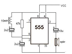
This metal detector electronic project schematic circuit is designed using a simple 555 timer integrated circuit. The schematic circuit requires few external electronic components. The metal detector circuit utilizes the 555 timer IC in an astable mode configuration, which generates...
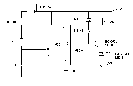
Just point this small device at the TV and the remote gets jammed. The circuit is self-explanatory. 555 is wired as an astable multivibrator for a frequency of nearly 38 kHz. This is the frequency at which most of...
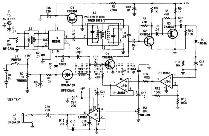
The integrated circuit Ul (an NE602 double-balanced mixer) functions as both an oscillator and a frequency mixer. Signals from the antenna input (at Jl) are transmitted through a DC-blocking capacitor C1 to the RF gain control, Rl, and subsequently...
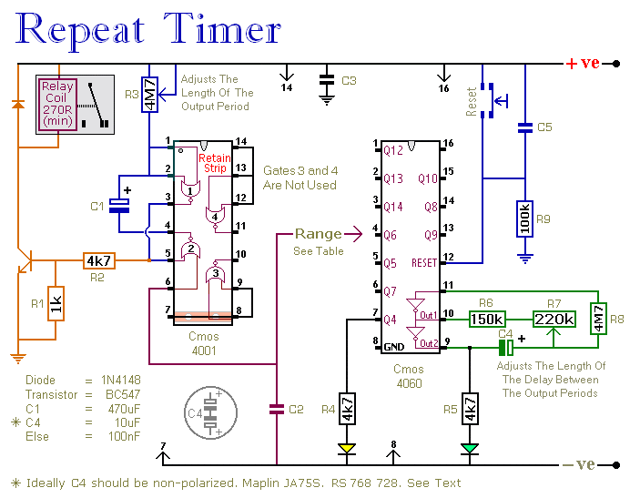
This circuit features an adjustable output timer that can re-trigger at regular intervals. The output duration can range from a fraction of a second to over half an hour, with the ability to recur at intervals from seconds to...
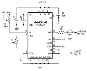
A high-frequency waveform generator is highly beneficial for electronic experimentation and design. This circuit generates sine wave oscillations; however, it can be modified to produce triangle or square wave functions. The frequency can be controlled using current. By disconnecting...
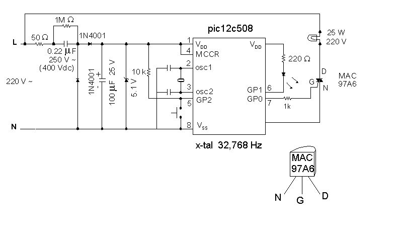
Introduction It is time for the 8-pin microcontroller Microchip PIC12C508, the SAVER V3.2, a new design of a device that controls a night light by turning it on and off. The SAVER V3.2 utilizes the Microchip PIC12C508 microcontroller, which features...