
Graphical Waveform Synthesiser

The circuit implementation is a CA3080 operating in the linear region. The differential input controls the magnitude and sign of the output current and hence the voltage slope between each fader. The programming current increases the gain of the integrator as the sample period decreases and thus keeps the output amplitude constant. The 1M feedback resistor gives some stabilization of the d.c. operating point. The offset control on the inputs is best used to adjust for minimum offset at highest programming current. The offset control on the output is used to compensate for leakage currents that cause the output to drift off at low programming currents. The input balance control allows the differential pot-downs to be set exactly equal so that square wave outputs are square and don't have ramps instead of flat tops. This is set at A440. The 10M resistor sets the waveform droop rate and is visible at very low operating frequencies. The output is d.c. coupled into the tracking filter minimizing signal droop. The FET buffer is essential and probably better than using a FET op-amp as there is minimal leakage and it is fast. If an LM13700 is used in this position, the on-board Darlington buffer takes too much input current and the corresponding output offset adjust resistor has to be too low value and causes the output to droop. Also, if compensating for offset changes by using two LM13700 sections with the inputs wired inversely, and taking the output difference, it is observed that the offsets of the two common die amps do not behave the same way at all. Tweaking the offset of one amp causes the other offset to vary radically.
On the next falling edge of U1 Q3, U1 count goes to 1. This selects fader 2 and fader 1, with U7 in the correct sense for the linear interpolator to create a ramp from voltage 1 to 2. The next rising edge of Q3 sets U2 to value 1 which selects fader 3 while U1 stays at fader 2, with U7 again changing state to switch the outputs to the correct input of the interpolator. The result is that the fader combinations 0-1, 1-2, 2-3, 3-4, etc., are presented to the inputs of the interpolator on each half clock cycle of HF_CLOCK.
The circuit design emphasizes a balance between precision and efficiency in the interpolation of analog signals, leveraging the capabilities of the CA3080 operational amplifier for dynamic control of voltage slopes. The incorporation of a clockless interpolation method reduces the complexity and potential timing issues associated with traditional clock-driven systems, enhancing the overall reliability of the circuit. The use of FET technology for buffering ensures low leakage and fast response times, which is critical in high-frequency applications. The feedback and offset adjustments are crucial for maintaining signal integrity, particularly in dynamic range applications where varying input conditions can lead to drift and inaccuracies. The design is intended for applications requiring precise voltage manipulation, such as in synthesizers or other audio processing equipment, where harmonic generation and accurate signal representation are paramount.Originally I intended to have 32 faders. Once I tried fitting them on a veroboard, 32 seemed rather excessive so I have reduced to sixteen. This still allows generation of accurate eigth harmonic which compares well with the Hammond's ninth harmonic. A MAX038 oscillator plus breakpoint circuit as in the Hammondicon was going to be my HF oscillator solution.
Good ol' Maxim seem to be incapable of producing any though, so I switched to a rather good transconductance triangle oscillator circuit which just about manages to get high enough in frequency with a clever compensation. Also, I originally used a resistor string and a switched system to interpolate between the fader voltages.
This required the clock to run very fast and was abandoned after a new clockless linear interpolator was devised. This sheet has the output connectors carrying the voltage from each fader to the second scanning board. The faders have each end of their travel connected to the +5V and -5V rails, so that each fader selects a voltage somewhere between these levels.
10uF capacitors on the wiper of each fader provide noise decoupling and a reservoir. Each fader is fed into the analogue switch bank. After reset, the switches both have "0" input values and thus select faders 0 and 1. The signal levels from faders 0 and 1 are fed through U7 and are then applied to each input of the linear interpolator. Q3 of U1 rising edge switches over the connections to each input of the interpolator and latches the current value of U1 onto U2 outputs.
At this point, U2 would normally have registered the previous count, but we have just had a reset so the outputs remain at zero. This involves a method of clockless linear interpolation between the fader steps. The pairs of fader voltages are presented at the two switch outputs in the correct order i.e. 0-1 then 1-2 then 2-3 etc. The voltage difference between these outputs represents a voltage proportional to the slope between the two points.
So if this voltage can be converted to a bipolar current and fed into a capacitor, the circuit will generate exactly such a straight line slope. The overall gain of the interpolator depends inversely on the capacitor value and the sample period, and directly proportionally to the voltage controlled current source transconductance.
This means that the output amplitude would normally reduce as the frequency increases, as the integrator naturally reduces output at -6dB per octave. This is cleanly compensated for by making the current source from a transconductance amp and increasing the programming current along with the oscillator CV and the tracking filter current drive.
The circuit implementation is a CA3080 operating in the linear region. The differential input controls the magnitude and sign of the output current and hence the voltage slope between each fader. The programming current increases the gain of the integrator as the sample period decreases and thus keeps the output amplitude constant.
The 1M feedback resistor gives some stabilisation of the d.c. operating point. The offset contol on the inputs is best used to adjust for minimum offset at highest programming current. The offset contol on the output is used to compensate for leakage currents that cause the output to drift off at low programming currents.
The input balance control allows the differential pot-downs to be set exactly equal so that square wave outputs are square and don't have ramps instead of flat tops. This is set at A440. The 10M resistor sets the waveform droop rate and is visible at very low operating frequencies. The output is d.c.coupled into the tracking filter minimising signal droop. You really do need these offset tweaks; There is no other way to do it. The FET buffer is essential and probably better than using a FET op-amp as there is minimal leakage and it is fast.
If you use an LM13700 in this position, the on-board Darlington buffer takes too much input current and the corresponding output offset adjust resistor has to be too low value and makes the output droop. Also if you try compensating for offset changes by using two LM13700 sections with the inputs wired inversely, and take the output difference, you find that...
1) The offsets of the two common die amps do not behave the same way at all. 2) Tweaking the offset of one amp makes the other offset vary radically. Not useful. I found this property most weird, and was convinced I had a wiring error. After extensive checking and getting desperate I rebuilt the circuit on a separate piece of board; Same result. I'm still not sure what was going on here as it seems improbable - but then there are no Nat Semi application circuits with offset adjusts on LM13700s.
Hmmm, makes you think. On the next falling edge of U1 Q3, though, U1 count goes to 1. This selects fader 2 and fader 1, with U7 in the correct sense for the linear interpolator to create a ramp from voltage 1 to 2. The next rising edge of Q3 sets U2 to value 1 which selects fader 3 while U1 stays at fader 2, with U7 again changing state to switch the outputs to the correct input of the interpolator.
The result is that the fader combinations 0-1 1-2, 2-3, 3-4, etc are presented to the inputs to the interpolator on each half clock cycle of HF_CLOCK. 🔗 External reference
Related Circuits
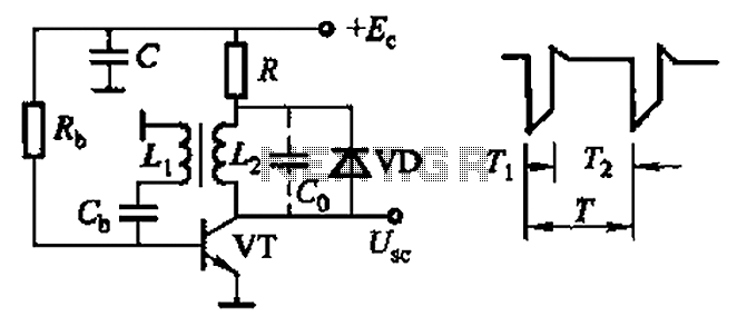
Common non-sinusoidal oscillator circuit, waveform and frequency formula - sawtooth oscillator - use blocking oscillator The sawtooth oscillator is a type of non-sinusoidal oscillator that generates a waveform characterized by a linear rise in voltage followed by a rapid drop....

The MC145152-2 synthesizer can be programmed using DIP switches, a diode matrix, or EPROM look-up tables. However, it is now difficult to find, costing around US$30. Modern synthesizers require PIC processors for programming or must remain connected to a...

An operational amplifier-based triangular waveform generator is a simple circuit that is widely used in function generators. This circuit utilizes the 741 operational amplifier to create a triangular wave generator. The output waveform of an integrator will be triangular...
The approaches using on-chip A-to-D converters on AVR, PIC, and Cypress controllers reached sample rates of up to about 60 kHz. Not really very useful for the sort of thing I was thinking about using this for: encoded data,...
These circuits are similar to that of Fig. 5-47, except that they provide for FM or sweep modulation. Circuit 5-50A is used for FM with small deviations, approximately ±10%. Circuit 5-50B is designed for a sweep range of 1000:1....
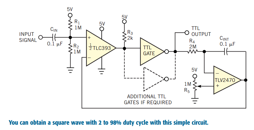
Converting periodic waveforms to square waves is an integral part of extracting a clock signal from data, creating waveform generators, and making timing-pulse generators. Any square-wave-conversion circuit is more valuable when the square wave's duty cycle is variable and...