
Hall Effect switch
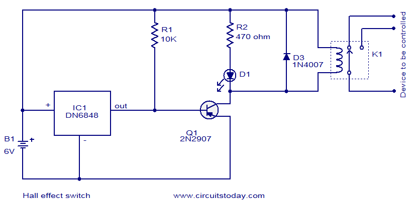
The Hall Effect switch circuit utilizes the DN6848 IC, which is designed to detect magnetic fields and translate this detection into a digital signal. The operation begins when a magnetic field, specifically the south pole of a magnet, is introduced near the sensor. This interaction causes the output pin (pin 3) of the DN6848 to drop to a low voltage, which is crucial for the subsequent operation of the circuit.
The PNP transistor Q1 is pivotal in controlling the relay's operation. When pin 3 of the DN6848 is low, Q1 turns ON, allowing current to flow through the relay coil. This energization of the relay coil closes the contacts, enabling the relay to control a larger load or activate other components within a circuit. The inclusion of resistor R1 is essential for maintaining the transistor in a stable state when no magnetic field is present, thus preventing false triggering due to noise or fluctuations in the environment.
The LED D1 serves as an indicator, providing a visual cue that the relay is activated. The current through the LED is regulated by resistor R2, which prevents excessive current that could damage the LED. Additionally, diode D2 is critical for protecting Q1 from back EMF generated when the relay coil is de-energized. This back EMF can create voltage spikes that may exceed the voltage ratings of the transistor, potentially leading to failure. The diode allows the induced current to safely dissipate, ensuring the longevity and reliability of the circuit.
Overall, this Hall Effect switch circuit is a robust solution for applications requiring non-contact sensing, leveraging the advantages of the DN6848 IC to provide a reliable and efficient means of detecting magnetic fields.The circuit diagram shown here is of a Hall Effect switch. Hall Effect sensor IC DN6848 from Panasonic is the heart of the circuit. The DN6848 has a built-in Hall Effect sensor, Schmitt trigger circuit, power supply regulator and temperature compensation circuits integrated to a single chip. High sensitivity, low drift and excellent temperature st ability of the DN6848 makes it well suitable for a variety of position, rotation and speed sensing applications. When the south pole of a magnet is brought near to the front face (face with type number marking) of the IC its output pin (pin 3) goes low (zero voltage).
The pin 3 is connected to the base of PNP transistor Q1 and the low stage at pin3 makes the transistor ON and makes the relay activated. In a nut shell the relay will get switched ON whenever the south pole of a magnet is brought close to the Hall Effect sensor IC DN6848.
Resistor R1 will always pull the base of Q1 to a very slight positive voltage and thereby prevents accidental triggering. LED D1 glows whenever the relay is activated and resistor R2 limits the current through the D1. Diode D2 is a freewheeling diode and it protects the transistor Q1 from high voltage spikes which are induced when the relay is switched.
🔗 External reference
Related Circuits

This power supply utilizes an SGS-Thomson UC3842 integrated circuit in an off-line flyback regulator configuration, delivering +5 V at 4 A and ±12 V at 300 mA. This design allows for the use of a compact high-frequency (50 kHz)...
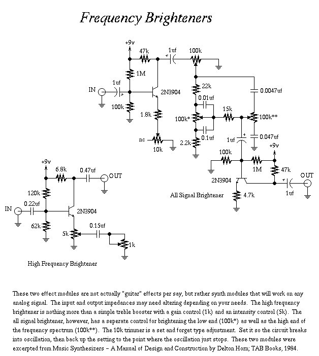
A collection of guitar fuzz, preamp, and operational amplifier (op-amp) electronic circuits and schematics designed for various guitar effects and distortion effects. This compilation includes a diverse range of electronic circuits that cater to guitarists seeking to enhance their sound...
This circuit can be integrated into a headlight switch to enable automatic switching between high and low beam headlights in the presence of oncoming traffic. It is a straightforward electronics project that includes a circuit diagram. The circuit operates by...
This 5-volt Switch Mode Power Supply circuit utilizes an integrated circuit (IC) from National Semiconductor, which specializes in the production and design of ICs for switch-mode power supply applications. The 5-volt Switch Mode Power Supply (SMPS) circuit is designed to...

A circuit configuration features a relatively new strong key touch-state switch. Normally, the thyristors VT1 and VT2 are in the off-state, allowing minimal current to pass through the lamp F. At this point, the capacitance C comes into play....

The circuit is complete, and the bulb is ON. To turn OFF the bulb from the upper switch at the top of the stairs, simply turn OFF the switch, which will break the circuit and turn the bulb OFF....