
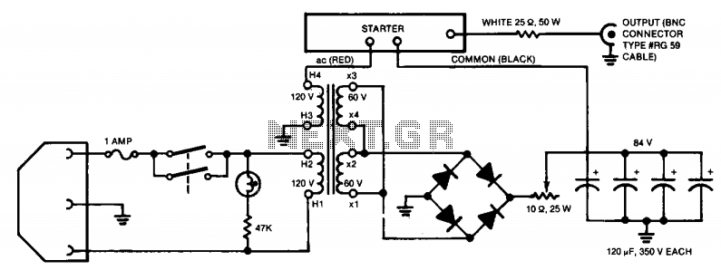
High current output switching power supply Schematic Diagram

The described circuit operates as a low voltage, high-current output switching DC power supply, designed to convert 220 volts AC input into a regulated DC output. The core of the circuit relies on a DIAC relaxation oscillator, which is crucial for initiating the conduction of the output switching transistor, designated as Q1. The role of Q1 is to control the flow of current to the load, and its on-time is managed by a timing and commutation network that includes Q2, C2, and an SCR. This network ensures that Q1 operates within a specific time frame, which is essential for maintaining consistent performance.
The output voltage remains stable and is largely unaffected by variations in the duty cycle, a significant advantage in applications where load conditions may change frequently. To further enhance the stability of the output voltage, the circuit incorporates an H11C optoisolator configured as a linear model unilateral PNP transistor. This component plays a vital role in the feedback loop, providing galvanic isolation while ensuring that any fluctuations in input voltage or load resistance are compensated for effectively.
The schematic diagram accompanying this description illustrates the arrangement of components and their interconnections, which are critical for the proper functioning of the power supply. The design emphasizes reliability and efficiency, making it suitable for various applications requiring stable high-current DC output.This is low voltage high-current ouput, switching dc power supplly wiht input 220 Volts AC, In this circuit, an St2 diac relaxation oscilator, Q3, C1, and the diac, initiates conduction of the output switching transistor Q1, the on time of which is maintained constant by a separate timing / commutation network consisting of Q2, C2, SUS, an d SCR 1. See schmeatic diagram below : The output voltage, consequently, is independent on the duty cycle. To compensate for unwanted variations of output voltage because of input voltage or load resistance fluctuations, an H11C wired as a liniear - model unilateral pnp transistor in a stable different amplifier configuration is connected into the galvanically isolated negative- feedback loop. You are reading the Circuits of High current output switching power supply And this circuit permalink url it is
🔗 External reference
Related Circuits
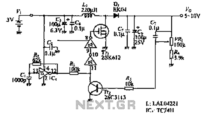
The design of the power supply circuit diagram utilizes an oscillator circuit from the 74HC series of CMOS logic circuits, with a MOSFET as the switching device. This configuration allows for the development of small-scale power supplies suitable for...
A dual-voltage circuit both initiates and sustains the arc. The lamps necessitate a starting voltage exceeding 1,000 volts. Once stable, the voltage across the lamp is approximately 20 volts. The power supply is divided into two primary sections. The...
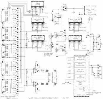
This circuit is not easy to build, but it provides excellent audio quality. It serves as a high-quality preamplifier, capable of driving high-quality power amplifiers while delivering good sound. The described circuit functions as a high-fidelity audio preamplifier, designed to...
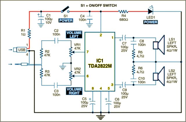
The circuit is designed as a dual audio power amplifier for use in battery-operated sound players. The TDA2822M specifications include low quiescent current, minimal crossover distortion, a supply voltage as low as 1.8 volts, and a minimum output power...
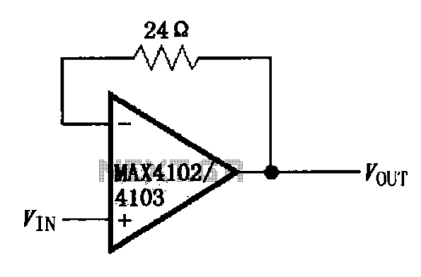
The MAX4102/4103 unity gain buffer circuit is illustrated in the figure. This circuit incorporates a small resistor (24 ohms) positioned in the feedback loop of the amplifier, which forms a unity gain buffer. Additionally, it achieves a maximum bandwidth...
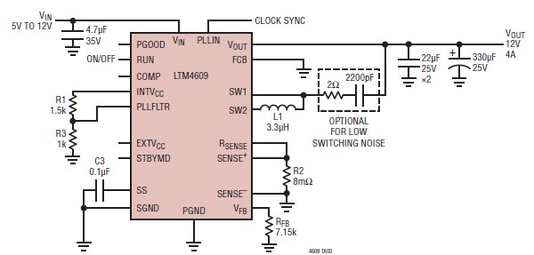
A very simple, high-efficiency switching mode buck-boost power supply circuit can be designed using the LTM4609 switching regulator IC. This circuit will provide a fixed output voltage of 12 volts. As illustrated in the schematic, the switching power supply...