
high frequency waveform generator

The waveform generator circuit typically utilizes a MAXIM IC, such as the MAX038, which is designed to generate various waveforms with high precision. The core functionality of the circuit revolves around the IC's ability to produce sine, triangle, and square waves by adjusting external components, such as resistors and capacitors, that set the frequency and amplitude of the output signals.
To create a sine wave output, the circuit employs a phase-locked loop (PLL) within the IC that generates a stable frequency. The output can be fine-tuned using a variable resistor or potentiometer, allowing for precise control over the waveform characteristics. For triangle and square wave outputs, additional configuration of the feedback loop and output stage can be implemented. This may involve integrating comparators and additional filtering stages to shape the waveform accordingly.
The circuit's power supply requirements should be considered, as the MAXIM IC typically operates within a specific voltage range. Proper decoupling capacitors should be placed close to the power pins of the IC to minimize noise and ensure stable operation.
Furthermore, the output stage may include buffer amplifiers to drive loads effectively without distortion. The design can also incorporate adjustable output levels and impedance matching components to suit various applications, such as testing audio equipment, simulating sensor outputs, or serving as a clock signal for digital circuits.
In conclusion, the waveform generator circuit based on a MAXIM IC is versatile and can be tailored to meet specific needs by modifying component values and configurations, making it an essential tool in electronic design and experimentation.This is the circuit of waveform generator. Waveform generator is very useful in electronic experiment and design. This circuit is generates sine wave oscillation, but actually we can modify the circuit to generate triangle or square wave function. This is the figure of the circuit. This circuit is based on MAXIM IC. This integrated circuit chip gi ves complete function to build a waveform generator/function generator. Here some of modifications that can be used to build a complete waveform generator circuit: 🔗 External reference
Related Circuits
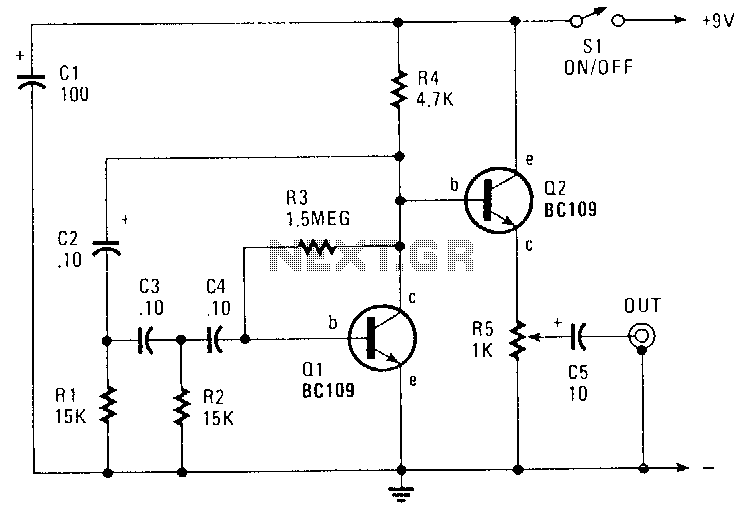
This circuit generates a sinusoidal output of approximately 8 V peak-to-peak, which can be adjusted down to zero, operating at a frequency of about 500 Hz. The signal is produced by a phase-shift oscillator. The described circuit utilizes a phase-shift...
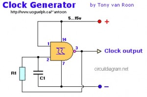
The following diagram represents a Clock Generator circuit that is constructed using NAND Gate logic integrated circuits (ICs). The circuit can utilize either IC 7400 or IC 4011. The 7400 is a TTL (Transistor-Transistor Logic) type, whereas the 4011...
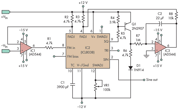
This basic voltage-controlled oscillator (VCO) and waveform generator integrated circuit (IC) circuit features a voltage follower loop (formed with IC1) and a symmetry feedback loop (IC3) designed to eliminate asymmetric duty cycles that can lead to distortion at low...
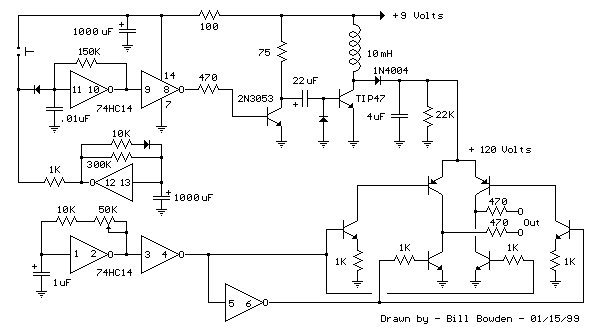
The telephone ring generator described generates the necessary aerial voltage using a simple switched-mode power supply (SMPS). It incorporates a CMOS Schmitt Trigger-based oscillator, a 10 mH inductor, a high-voltage switching transistor (such as the TIP47 or another high-voltage,...

The divider design is straightforward. Users can select a division factor of 1, 10, or 100, or opt for no output (tied low) through the CONTROL input connected to the analog multiplexer HC4052. The design utilizes AC04 to drive...
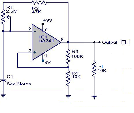
A square wave generator using the UA741 integrated circuit is presented. This circuit employs positive feedback for Schmitt trigger action and negative feedback to measure the waveform timing. Initially, it is assumed that the output is high and capacitor...