
HIGH-SPEED DIGITAL DESIGN

The circuit design focuses on high-speed digital communication, emphasizing the importance of transmission line characteristics and impedance control to minimize signal integrity issues. The stacking of layers in the PCB is critical for optimizing the performance of the transmission lines, which must be carefully calculated to ensure that the characteristic impedance matches the requirements of the components used, particularly in high-speed applications. The moated ground area surrounding the crystal oscillator serves to isolate high-frequency noise, enhancing the stability of the oscillator and the overall circuit performance.
Pin/gate swapping is a technique employed to optimize the routing of signals on the PCB, facilitating a more efficient layout that can reduce trace lengths and improve signal integrity. The heat spreader design, utilizing vias to connect to the ground plane, aids in thermal management, ensuring that heat generated by the components is effectively dissipated, thereby maintaining operational reliability.
The microcontroller/digital signal processor (uP-EXD10) operates at a clock frequency of 66 MHz, making it suitable for applications requiring rapid data processing. The FO-TX interface IC enables the conversion of electrical signals to optical signals, facilitating communication over fiber optic cables. The inclusion of the fiber-optic laser diode (LD1) is essential for transmitting these optical signals, while the 54ALS00 NAND gates provide necessary logic functions for input/output operations, ensuring compatibility with various digital signal levels.
Overall, this example serves as a practical reference for designing high-speed digital PCBs, demonstrating key techniques and considerations for achieving optimal performance in modern electronic applications.This example demonstrates how to stack up layers and design transmission lines for a high-speed digital PCB. The example also demonstrates how to create a moated ground area with a bridge around a high-frequency crystal oscillator, how to perform pin/gate swapping, and how to create a heat spreader using vias to the Ground plane.
The example circu it is shown in Figure 9-156. The BOM for this example is shown in Table 9-8. The circuit consists of a (fictional) high-speed, low-pin-count microcontroller/digital signal processor (uP-EXD10) driven by a 66-MHz clock (X1), a digital to fiber optic interface IC (FO-TX, which mimics an ADN2530 but with fewer pins), a fiber-optic laser diode (LD1), and a couple of 54ALS00 NAND gates used for I/O decoding. The digital signals have rise and fall times from 200 ps to 1. 9 ns and require controlled impedance traces (see the Analog Devices ADN2530 data sheet for an example application).
In a real design, more bypass capacitors would be used on the circuit, but the design is scaled down to keep the design simple. The parts and footprints are located on the Web site for this book. 🔗 External reference
Related Circuits
For beginners in microcontroller projects who are unsure where to start, this project serves as one of the simplest options available. It provides a clear understanding of programming a microcontroller. Often, one may glance at a watch and ponder,...

The LM2876 audio power amplifier circuit can be designed as a simple, high-efficiency audio amplifier capable of delivering 40W of continuous average power to an 8-ohm load with a total harmonic distortion plus noise (THD+N) of 0.1% from 20Hz...
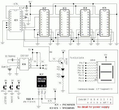
The diagram illustrates a block diagram for an agenda alarm and agenda thermometer system. It includes one temperature sensor, a real-time clock (RTC), a microcontroller (PIC), an EEPROM, a 7-segment display, and a keyboard. The EEPROM is utilized to...
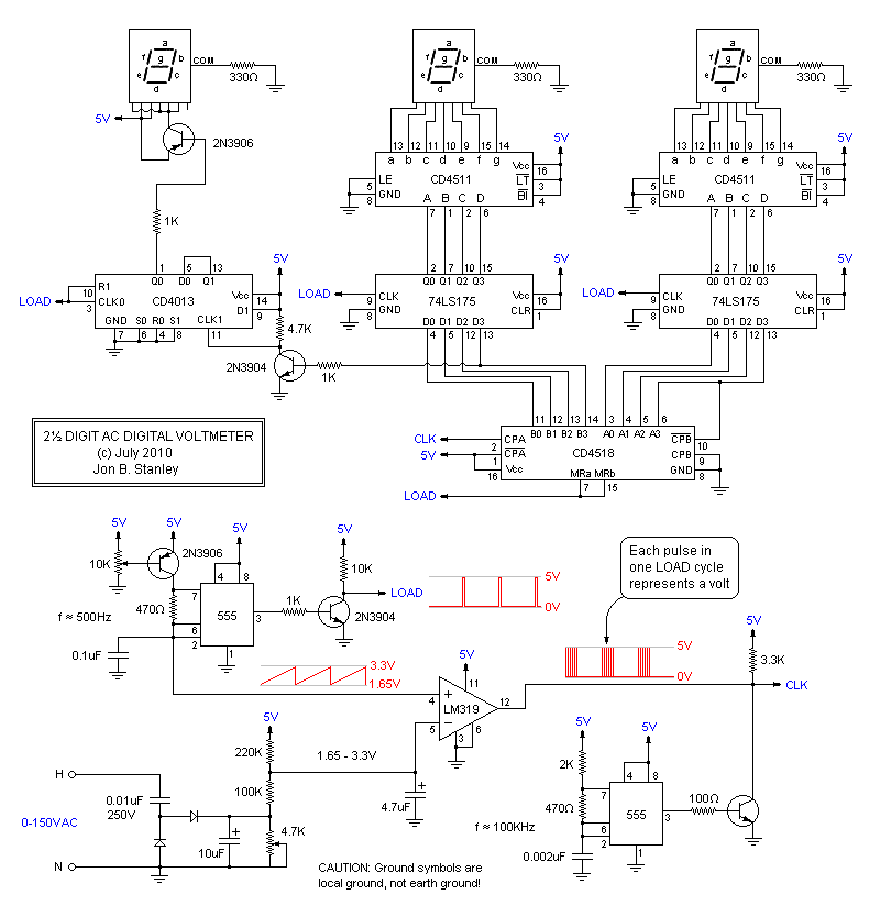
The project began as a simple variac (variable autotransformer) and electrical outlet mounted on a wooden block. Eventually, it was housed in the case of an old audio signal generator for improved safety and aesthetics. A 0-250VAC analog meter...

This constant gain, constant Q, variable frequency filter provides simultaneous low-pass, bandpass, and high-pass outputs. With the specified component values, the center frequency will be 235 Hz for high logic inputs and 23.5 Hz for low logic inputs. The...
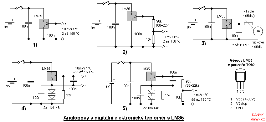
The electronic thermometer has numerous applications. Standard mercury thermometers cannot be used everywhere due to their size, fragility, or the need for remote measurement. The advantages of electronic thermometers include their compact size, low heat capacity of probes, faster...