Lie detector

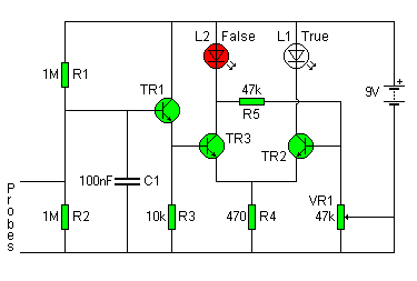
The circuit diagram of the Lie Detector is illustrated above. It consists of three transistors (TR1 to TR3), a capacitor (C1), two lights or LEDs (L1 & L2), five resistors (R1 to R5), and a variable resistor (VR1). This circuit operates on the principle that a person's skin resistance changes with perspiration, which can occur when they are not truthful. The resistance of dry skin is approximately 1 million ohms, while moist skin can reduce this resistance by a factor of ten or more. Resistors R1 and R2 create a voltage divider, each with a resistance of 1,000,000 ohms (1 mega ohm). Due to their equal values, the voltage at the upper probe wire is half the battery voltage (approximately 4.5 volts). When an individual holds the probe wires, their skin resistance alters the voltage at the upper probe wire. The skin resistance is in parallel with R2, and since it is likely to be equal to or lower than R2, the voltage at the probe wire decreases as skin resistance decreases. TR1 and R3 form a buffer circuit known as an emitter follower. The voltage at the emitter of TR1 mirrors the voltage at the probe wire, allowing it to drive transistor TR2. Transistors TR1 and TR2 function as a voltage comparator. If the voltage at the base of TR2 exceeds that at the base of TR3, the green LED (L1) will illuminate. Conversely, if the voltage at the base of TR3 is higher, the red LED (L2) will light up. To operate the Lie Detector, grasp the probe wires and adjust VR1 until the green LED is barely illuminated and the red LED is off. This adjustment indicates that the voltage at the base of TR2 is just greater than that at the base of TR3. Using moist fingers to hold the probes will lower the skin resistance, causing the voltage at the base of TR2 to drop. Consequently, the voltage at the base of TR3 will be greater, activating the red LED.
The Lie Detector circuit is designed to measure variations in skin resistance, which can indicate physiological responses associated with deception. The circuit employs three transistors for signal amplification and comparison, ensuring that even slight changes in skin resistance can be detected. The voltage divider formed by R1 and R2 is critical for establishing a reference voltage, which is necessary for the comparator function of TR1 and TR2. The emitter follower configuration of TR1 provides a high input impedance, allowing it to effectively read the voltage from the probe wires without loading the circuit, thus maintaining accuracy in the readings.
The use of two LEDs serves as a visual indicator of the state of the lie detection process. The green LED signals a baseline or truthful response, while the red LED indicates a potential deceptive response. The variable resistor VR1 allows for calibration of the circuit to account for individual differences in skin resistance, ensuring that the system remains sensitive and accurate across different users.
Overall, this circuit is a practical application of basic electronic principles to create a device capable of interpreting human physiological responses, demonstrating the intersection of electronics and psychology in detecting deception.The circuit diagram of the Lie Detector is shown above. It consists of three transistors (TR1 to TR3), a capacitor (C1), tw1o lights or LEDs (L1 & L2), five resistors (R1 to R5), and a variable resistor (VR1). This circuit is based on the fact that a person`s skin resistance changes when they sweat (sweating because they`re lying).
Dry skin has a resistance of about 1 million ohms, whereas the resistance of moist skin is reduced by a factor of ten or more. Resistors R1 and R2 form a voltage divider. They have resistances of 1 000 000 ohms (1 mega ohms) and, because their values are equal, the voltage at the upper probe wire is half the battery voltage (about 4.
5 volts). A person holding the probe wires will change the voltage at the upper probe wire depending on their skin resistance. The skin resistance is in parallel with R2 and, because it is likely to be similar to or smaller than R2, the voltage at the probe wire will fall as skin resistance falls.
TR1 and R3 form a buffer circuit (called an emitter-follower). The voltage at the emitter of TR1 follows the voltage at the probe wire and is now able to drive transistor TR2. Transistors TR1 and TR2 act as a voltage comparator. If the voltage at the base of TR2 is higher than at the base of TR3 then the green LED (L1) will come on.
If the reverse is true then the red LED (L2) will light. To test the Lie Detector hold the probe wires. Adjust VR1 until the green LED is just on and the red LED is just off. This is the point at which the voltage at the base of TR2 is just greater than at the base of TR3. Now use moist fingers to hold the probes. This lowers the skin resistance and causes the voltage at the base of TR2 to fall. The voltage at the base of TR3 is now greater and the red LED comes on. 🔗 External reference


