
Line driver provides full rail excursions

The circuit described employs opto-isolators U1 and U2 to achieve electrical isolation between the logic input and the output stage. The npn and pnp configurations of the emitter followers ensure that the output signals are appropriately conditioned for the subsequent stages. Potentiometer R2 provides a means to fine-tune the DC balance, allowing for precise control over the output characteristics.
The complementary TMOS pair, consisting of Q1 and Q2, is driven by the emitter followers, enabling efficient switching and amplification of the input signal. The ±12 V supply provides a nominal output swing of about 12 V peak-to-peak, which is suitable for many applications. However, the inclusion of a ±18 V boost circuit enhances the output capability, allowing the swing to approach the supply rails, thus maximizing the available voltage range for downstream components.
The output from the TMOS pair is routed to transformer T1, which serves to step up or step down the voltage as required by the application. The diode bridge D3 rectifies the AC output from the transformer, converting it into a usable DC voltage. This rectified voltage is then regulated by voltage regulators U3 and U4, ensuring a stable output voltage for the collectors of the opto-isolators.
Diodes D1 and D2 play a critical role in the circuit's operation, providing protection and ensuring proper biasing under different supply conditions. When operating with the 12 V supply, these diodes are forward-biased, allowing current to flow and maintain the necessary operating conditions. Conversely, when the 18 V boost is activated, D1 and D2 become back-biased, preventing any unwanted current flow that could disrupt the circuit's functionality.
Overall, this circuit design effectively combines opto-isolation, amplification, and voltage regulation to produce a reliable output suitable for various electronic applications.The logic input is applied to opto-isolators Ul and U2 with, respectively, npn and pnp emitter follower outputs. Dc balance is adjusted by potentiometer R2. The emitter followers drive the gates of Ql and Q2, the complementary TMOS pairs. With a ±12 V supply, the swing at the common source output point is about 12 V peak-to-peak. By adding a ± 18-V boost circuit, as shown, the output swing can approach the rail swing. This circuit applies the output to transformer Tl, which is rectified by diode bridge D3, regulated by U3 and U4, and then applied to the collectors of Ul and U2. Diodes Dl and D2 are forward-biased when 12-V supplies are used, but they are back-biased when the 18-V boost is used.
Related Circuits

The circuit diagram illustrates a simple stepper motor controller utilizing basic components. The driver circuit employs four SL100 transistors to control the motor windings, along with two NOT gates and one XOR gate to decode the two-bit control logic...
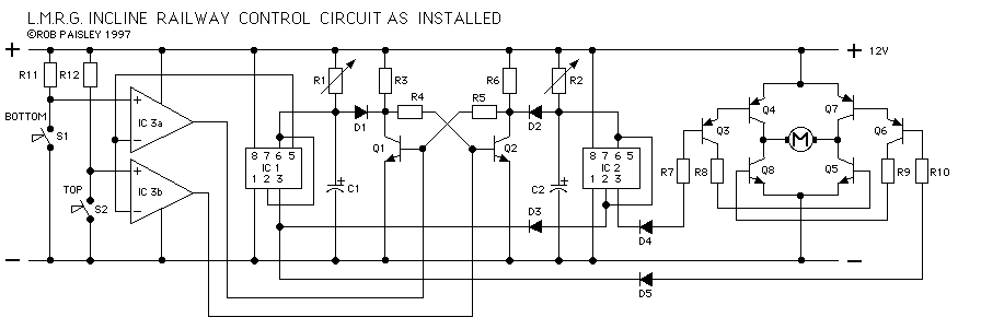
The drawings and photos below are for an operating incline railway that was built by the London Model Railroad Group for its O scale model railway club located at London, Ontario, Canada. This is a single car model loosely...
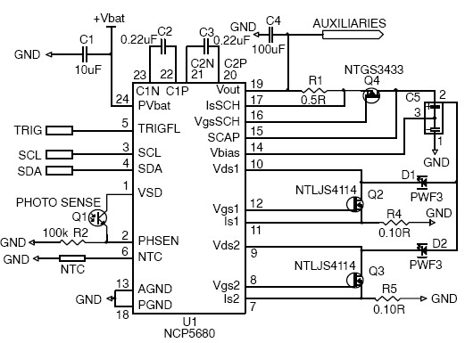
This white LED driver circuit project utilizes the NCP5680 high-efficiency white LED driver integrated circuit (IC). The NCP5680 supports dual power flash LED and torch operations. Its built-in DC/DC converter employs a highly efficient charge pump structure with operating...
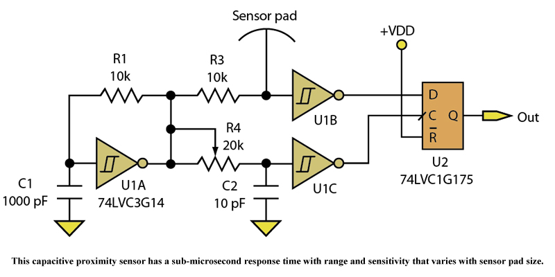
Three devices in a quad Schmitt Trigger and a Flip-Flop create a simple yet sensitive proximity sensor. The described circuit utilizes three devices from a quad Schmitt Trigger configuration alongside a Flip-Flop to construct a proximity sensor. The Schmitt Trigger...
The following diagram is for the main circuit of the motor driver. A testing version is shown near the end of this page. It is laid out differently and shows the SN7474 in logic block form and LEDs are...
The transformer is a 220V to 12V, 50Hz, and 3.6VA PCB type transformer. The model depicted is HRDiemen E3814056. Being encapsulated, it is isolated from external influences. A 250V 400mA glass fuse protects the circuit from damage caused by...