
LM5020 High Voltage - Speed PWM Controller

The LM5020 is a versatile integrated circuit designed for use in power supply applications. It incorporates various features that enhance its performance and reliability.
The connection diagram of the LM5020 illustrates how the device interfaces with other components in a power supply circuit. It typically includes input and output pins, control pins for enabling or disabling the device, and feedback pins for voltage regulation. Understanding the pin descriptions is crucial for proper circuit design, as each pin has a specific function that contributes to the overall operation of the device.
The functional block diagram provides a high-level view of the internal architecture of the LM5020. It shows the arrangement of key components such as the internal high-gain error amplifier, which is responsible for maintaining output voltage stability by comparing the feedback voltage to a reference voltage. The error amplifier adjusts the duty cycle of the switching transistor to regulate the output voltage effectively.
The line under voltage lockout (UVLO) circuit is a protective feature that prevents the LM5020 from operating under low input voltage conditions, which could lead to unstable performance or damage. This circuit monitors the input voltage and disables the device if it falls below a predetermined threshold, ensuring safe operation.
The cycle-by-cycle overcurrent protection function is another critical feature of the LM5020. This mechanism detects overcurrent conditions in real-time and limits the output current by adjusting the duty cycle of the switching signal. This protection helps prevent overheating and damage to the power supply and connected components.
The oscillator frequency of the LM5020 is adjustable, allowing designers to optimize the switching frequency for their specific application. This flexibility can improve efficiency, reduce electromagnetic interference (EMI), and enhance overall performance.
Lastly, the duty cycle limit options provide additional control over the maximum duty cycle of the switching signal. This feature is essential for ensuring that the power supply operates within safe limits, particularly in applications where load conditions may vary significantly.
In summary, the LM5020 integrates multiple functionalities that make it suitable for various power supply designs, with essential features such as voltage regulation, protection mechanisms, and frequency adjustment capabilities. Understanding these elements is crucial for effective implementation in electronic circuits.find sections such LM5020 Connection Diagram and pin descriptions, the functional block diagram of the device, line Under Voltage Lock Out (UVLO) circuit, an internal high gain error amplifier, a cycle-by-cycle over current protection function, sets the LM5020 oscillator frequency, and The LM5020 duty cycle limit options 🔗 External reference
Related Circuits
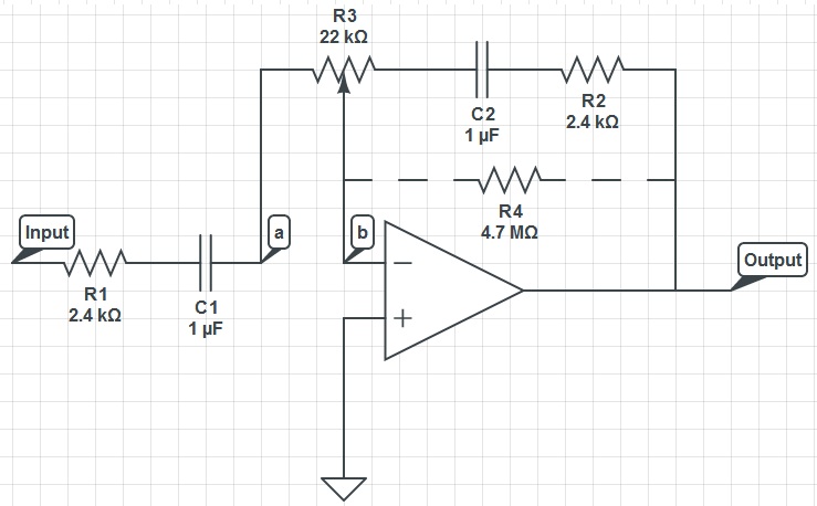
This circuit can function as a treble control circuit, with high-frequency gain occurring when resistor R3 is set to a value that makes points a and b equal (denoted as k=0). Conversely, high-frequency attenuation occurs when R3 is set...
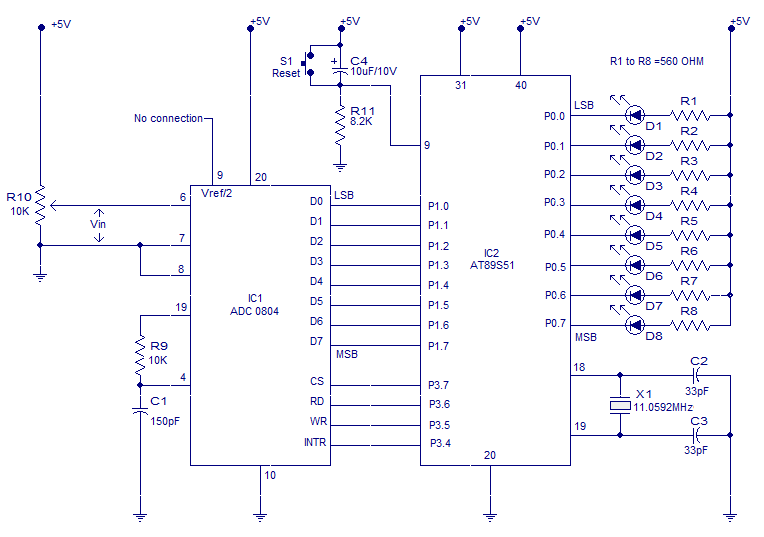
Interfacing ADC to 8051 microcontroller. ADC0804 is interfaced to microcontroller AT89S51. Complete circuit, theory and program in assembly language. The interfacing of an Analog-to-Digital Converter (ADC) with a microcontroller is a critical aspect of embedded systems design, particularly when analog...

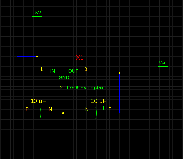
The 5 volt regulated power supply for TTL and 74LS series integrated circuits has to be very precise and tolerant of voltage transients. These ICs are easily damaged by short voltage spikes. A fuse will blow when its current...
The voltage to frequency converter (V/FC - VCO) circuit consists of a UJT (uni-junction transistor) oscillator in which the timing charge capacitor C2 is utilized. The voltage to frequency converter circuit operates by converting an input voltage into an output...
The "R-h sampling circuit limit order" aims to reduce the sampling resistor. A DC voltage level can be positioned between the components. The circuit includes a line amplifier that allows for magnification adjustments and is designed to protect against...
A PIR sensor is triggered when using a timer to wait for 2 seconds after the sensor is activated. Without the timer, the sensor operates as intended. The PIR sensor is connected to an ATMega328p microcontroller, which has three...