
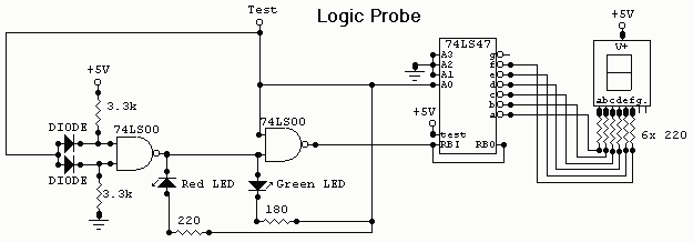
LOGIC PROBE

The versatile logic probe is designed to provide a simple and effective means for troubleshooting digital circuits. It operates by detecting and indicating the logic levels of the signals present at various points in a circuit. The core of the probe consists of two inverters from the 7404 IC, which serve to amplify the input signal and provide a clean output that can be easily interpreted.
The inclusion of a zener diode (D1) is a critical feature that protects the input of the probe by clamping the voltage to a safe level, specifically just above the 2.2-V threshold of TTL logic. This ensures that higher voltages do not damage the sensitive components of the probe when interfacing with various circuit voltages. If the probe is exclusively used with TTL circuits, the zener diode can be excluded, simplifying the design without compromising functionality.
In addition to the inverters, the schematic may include other passive components such as resistors and capacitors that help stabilize the circuit and filter out noise. The output of the logic probe is typically connected to an LED or a similar indicator, which illuminates to signify the presence of a high or low logic level. This visual feedback allows engineers and technicians to quickly assess the operational status of digital signals during testing and debugging processes.
Overall, the design of the logic probe emphasizes versatility and ease of use, making it an essential tool for anyone working with digital electronics. Its straightforward construction and effective signal detection capabilities make it suitable for a wide range of applications in both educational and professional settings.The figure shows the schematic for a versatile logic probe. The zener diode clamps the input signal just above the TTL inverter`s 2.2-V trigger voltage. Zener diode D1 can be left out if the probe is going to be used only on TTL circuits. The logic probe is based mainly on inverters IC1-a and IC1-b, which are sections of a 7404 integrated circuit. Depending.. 🔗 External reference
Related Circuits
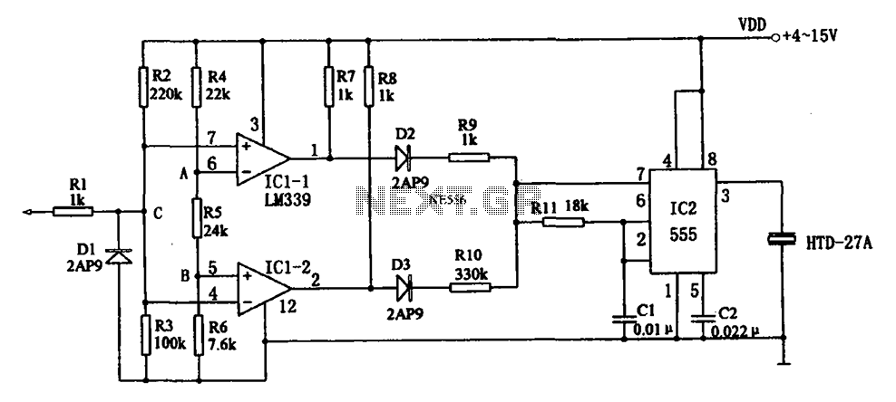
The acoustic logic level probe circuit consists of a voltage comparator, multivibrator, piezoelectric ceramics (HTD), and other components. The configuration of the audio circuit determines the frequency of the sound level to assess the logic levels of TTL or...
This circuit is a Logic Probe. It indicates the logic state of the node of any TTL logic circuit. To do that, we have to supply the probe with the same power of the circuit that we want to...
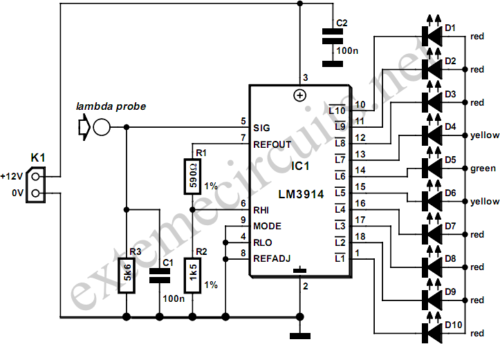
A lambda probe, also known as an oxygen sensor, is commonly found on the exhaust systems of vehicles that operate on unleaded fuel. Once it reaches its normal operating temperature of approximately 600 degrees Celsius, the lambda probe generates...
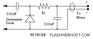
An RF probe is used to directly measure the level of RF voltage present at a particular point and is one of the most useful test instruments in the hands of the home brewer. It is normally used with...

The pulser generates pulses at a user-selected frequency of 0.5 or 500 Hz, with a pulse width of about 5 ms. If the input to be pulsed is already being driven high or low by another output, the pulser...
This FET probe features an input impedance of 10 MΩ, which is shunted by 8 pF. Removing the protective diodes reduces this impedance to approximately 4 pF. The frequency response of the probe ranges from DC to 20 MHz...