
Long duration timer circuit

The timer circuit operates on a principle of time delay generated by the combination of resistor R1 and capacitor C1. The timing period is determined by the RC time constant, which is calculated as τ = R1 × C1. In this circuit, the values of R1 and C1 must be selected to achieve the desired delay of approximately 35 minutes. A typical configuration might involve a resistor in the range of several megaohms and a capacitor in the range of microfarads.
Upon pressing switch S2, the circuit initiates the timing sequence. The discharge of capacitor C1 through R1 causes the voltage across C1 to drop. The NAND gates within the CMOS IC 4011 are configured in such a way that when their inputs are at logic low (0V), the outputs transition to logic high, providing the necessary signal to turn on transistor Q1. The transistor acts as a switch for the relay, allowing current to flow through the relay coil, thus energizing the relay contacts and powering the connected device.
The release of switch S2 allows capacitor C1 to charge through R1. As the capacitor charges, the voltage rises until it reaches half of the supply voltage, which is the threshold for the NAND gates. At this point, the outputs of U1 revert to low, turning off transistor Q1 and deactivating the relay. The relay contacts open, disconnecting power from the appliance.
Switch S1 provides a manual override feature, allowing the user to interrupt the timing sequence and turn off the connected device at any point before the timer completes its cycle. This feature enhances user control over the operation of the timer circuit, making it versatile for various applications where automatic shut-off is beneficial.
In summary, this timer circuit effectively combines simple components to create a reliable and energy-saving solution for automatic appliance control. Its design leverages the properties of CMOS technology and passive components to achieve a long time delay, making it suitable for a variety of household and industrial applications.This timer circuit can be used to switch OFF a particular device after around 35 minutes. The circuit can be used to switch OFF devices like radio, TV, fan, pump etc after a preset time of 35 minutes. Such a circuit can surely save a lot of power. The circuit is based on quad 2 input CMOS IC 4011 (U1). The resistor R1 and capacitor C1 produces the required long time delay. When pushbutton switch S2 is pressed, capacitor C1 discharges and input of the four NAND gates are pulled to zero. The four shorted outputs of U1 go high and activate the transistor Q1 to drive the relay. The appliance connected via the relay is switched ON. When S2 is released the C1 starts charging and when the voltage at its positive pin becomes equal to ½ the supply voltage the outputs of U1 becomes zero and the transistor is switched OFF.
This makes the relay deactivated and the appliance connected via the relay is turned OFF. The timer can be made to stop when required by pressing switch S1. 🔗 External reference
Related Circuits
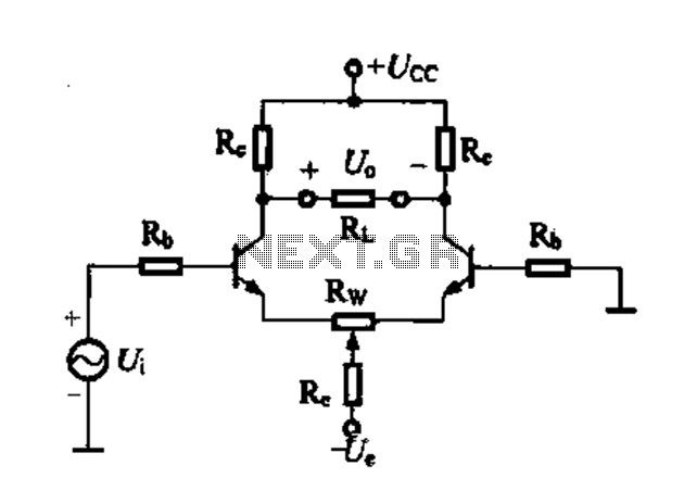
Differential amplifier circuit with four connection methods and characteristics for comparison. The circuit exhibits magnification with a single tube when symmetrical. Additionally, CMRR (Common Mode Rejection Ratio) is adapted from single-ended input to a double-ended output. The differential amplifier is...
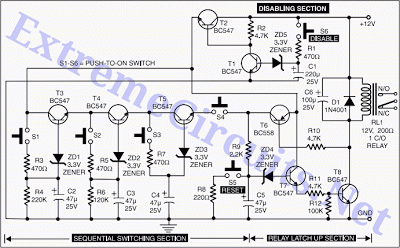
This intelligent electronic lock circuit is constructed using only transistors. To unlock this electronic lock, the user must press tactile switches S1 through S4 in sequence. For added security, these switches can be labeled with different numbers on the...

This board layout was created using the SOIC version of a PIC16F627A without drawing the usual schematic first. Most of the part values are etched on the Layout. The SIP resistor packs I used are 10k ohm, some experimentation...
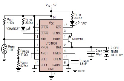
The LTC4060 integrated circuit can be utilized to create a straightforward smart NiMH battery charger electronic project. This charger circuit functions as a complete fast charging system for NiMH or NiCd batteries. It requires only a few external components...
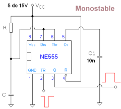
The 555 Timer is an integrated circuit utilized for various functions such as timing, pulse generation, and tone generation, all from a single universal IC. Each pin's function is detailed, and design recommendations are provided as necessary. A Monostable...

This circuit illustrates a simple boost converter, which is powered by an oscillating signal generated by the NE555 timer. The signal is amplified through a VT transistor to drive a booster transformer. This step-up transformer increases the oscillating signal,...