
Low-distortion 1.6-30mhz ssb driver

The amplitude of the out-of-phase voltages at the bases is inversely related to frequency due to the series inductance in the feedback loop and the increasing input impedance of the transistor at lower frequencies. In contrast, the negative feedback reduces the effective input impedance presented to the source (distinct from the device's own input impedance), and with the correct voltage slope, it can be equalized. This method enables the maintenance of an input voltage standing wave ratio (VSWR) of 1.5:1 or less, up to 30 MHz.
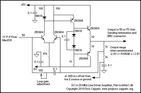
The described amplifier circuit is designed for efficiency and performance, particularly in RF applications. The use of MRF476 and MRF475 transistors allows for robust operation, ensuring minimal distortion and high linearity. The adjustable bias currents facilitate fine-tuning of the amplifier's performance, accommodating variations in component tolerances and operating conditions. The capacitors employed for audio-frequency bypassing are critical in maintaining signal integrity and minimizing unwanted feedback that could adversely affect performance.
The RC networks used for gain leveling are strategically placed to provide a smooth response across the operating frequency range. This design choice is essential for applications requiring consistent gain characteristics, particularly in communication systems where signal fidelity is paramount. The negative feedback mechanism not only improves stability but also enhances the amplifier's ability to handle varying load conditions without significant degradation in performance.
Overall, this amplifier design exemplifies a careful balance between cost-efficiency and high-performance metrics, making it suitable for a wide range of applications in the RF spectrum. Proper implementation of this circuit can yield reliable operation with minimal maintenance, making it an attractive option for both commercial and amateur radio applications.The amplifier provides a total power gain of about 25 dB, and the construction technique allows the use of inexpensive components throughout. The MRF476 is specified as a 3 watt device and the MRF475 has an output power of 12 watts. Both are extremely tolerant to overdrive and load mismatches, even under CW conditions. Typical IMD numbers are better than -35 dB, and the power gains are 18 dB and 12 dB, respectively, at 30 MHz.
The bias currents of each stage are individually adjustable with R5 and R6. Capacitors C4 and CIO function as audio-frequency bypasses to further reduce the source impedance at the frequencies of modulation. Gain leveling across the band is achieved with simple RC networks in series with the bases, in conjunction with negative feedback.
The amplitude of the out-of-phase voltages at the bases is inversely proportional to the frequency as a result of the series inductance in the feedback loop and the increasing input impedance of the transistor at low frequencies. Conversely, the negative feedback lowers the effective input impedance presented to the source (not the input impedance of the device itself) and with proper voltage slope would equalize it.
With this technique, it is possible to maintain an input VSWR of 1.5:1 or less than 1.6 to 30 MHz.
Related Circuits

This is an efficient flyback driver for modern cylindrical rectified television flybacks. Many sites do not provide circuits for driving these transformers; they simply state that they are ineffective. However, this circuit has been built and tested, focusing on...
The output cable from my 20 MHz function/sweep generator dangled over the side of the workbench, the alligator clip hovering over the floor. Deeply engrossed in a project, I moved the power strip on the floor a little closer...
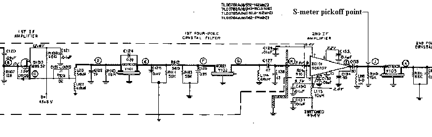
The artwork style of the operational amplifier and the meter face suggests that it is an ACC design from an old issue of ACC Notes. The second image was scanned, and the text below was written from scratch. If...
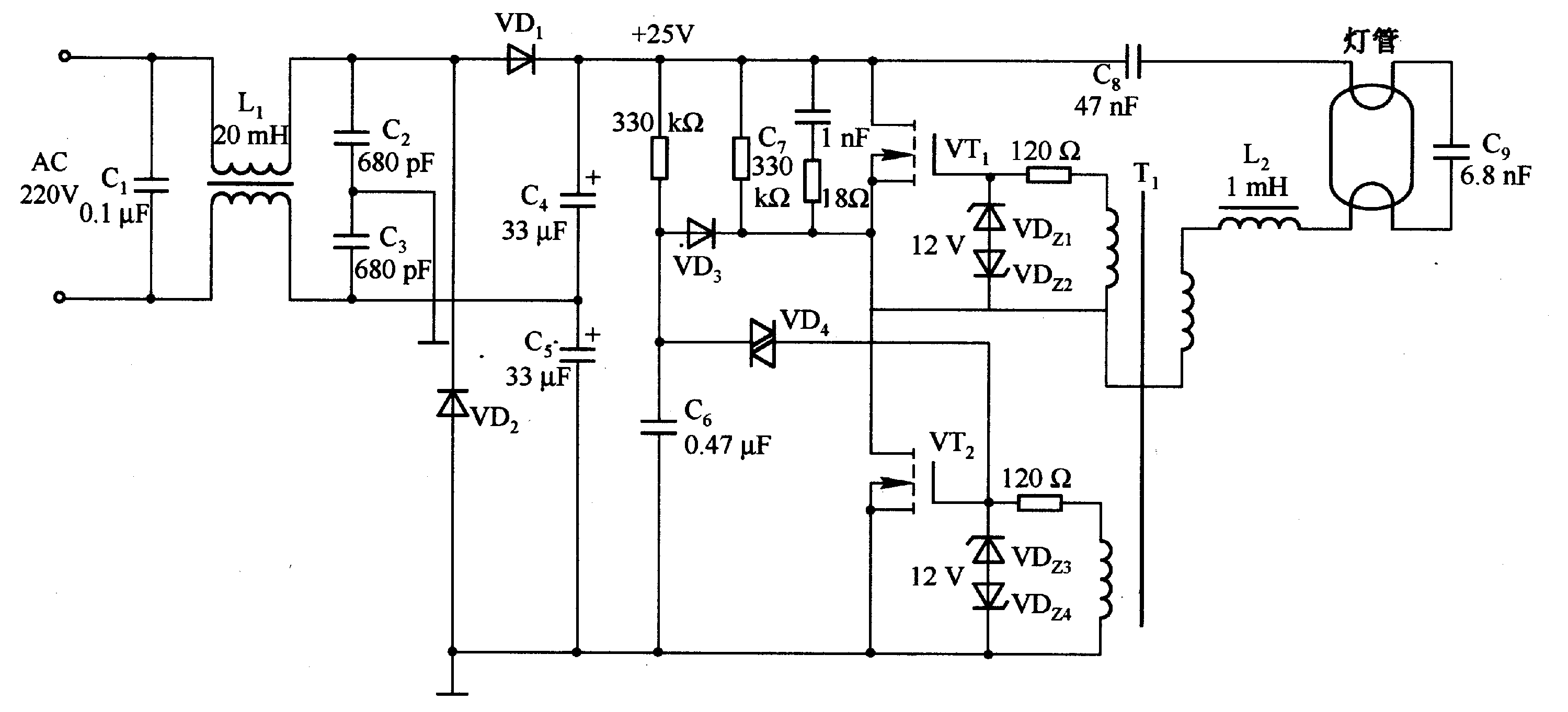
A fluorescent tube is connected in an LC resonant circuit consisting of inductor L2 and capacitor C9. The bidirectional breakdown diode VD4 initiates the starting circuit. When AC power is applied, the gate potential of transistor VT2 increases due...
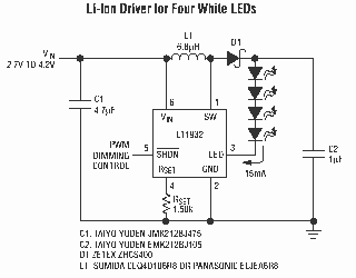
The LT1932 is a fixed frequency step-up DC/DC converter designed to operate as a constant-current source. Because it directly regulates output current, the LT1932 is ideal for driving light emitting diodes (LEDs) whose light intensity is proportional to the...
Need more current? If you have a larger motor ready for use, the Pololu High Current Motor Driver Board 14A 6V-16V is the ideal solution. Connect three digital lines to your microcontroller (five if error condition feedback is desired),...